Preparation method of ceramic substrate for medium-free copper-coated gold-deposited light-emitting diode (LED) package

A technology of LED packaging and copper immersion gold, which is applied in the direction of electrical components, circuits, semiconductor devices, etc., can solve the problems of not meeting the requirements of high-power current passing, electrophoretic effect, poor ceramic bonding force, etc., and improve the long-term maintenance rate , solve the problem of vulcanization, the effect of excellent thermal conductivity

Inactive Publication Date: 2016-04-13
郭垣成
View PDF3 Cites 2 Cited by
  • Summary
  • Abstract
  • Description
  • Claims
  • Application Information

AI Technical Summary

Problems solved by technology

The electroplating method is first to metallize the ceramics. During the production process, a large amount of harmful sewage will be generated, polluting the environment, and the deposited film layer is extremely thin, so it needs to be thickened by multiple layered electroplating, and a large amount of harmful sewage will be generated again during the electroplating process. Sewage; and this electroplating deposition coating film also has disadvantages such as poor toughness, poor bonding force with ceramics, easy fall off of electrode points, and poor current passing ability of thin coating film, which cannot meet the requirements of high-power current passing.
[0003] The ceramic substrates currently used in LED products use printed silver paste circuits. Silver paste has inherent disadvantages of vulcanization. After vulcanization, the surface becomes black, which directly affects the refractive index of light. The increase will lead to an increase in the voltage of the product, which will increase the heat generation and eventually lead to product failure.

Method used


Image

  • Preparation method of ceramic substrate for medium-free copper-coated gold-deposited light-emitting diode (LED) package

Examples


Embodiment 1

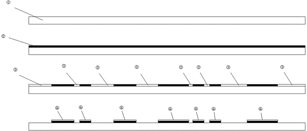
[0017] see figure 1 , in an embodiment of the present invention, a manufacturing process of a dielectric-less copper immersion gold-clad LED packaging ceramic substrate, the specific steps are as follows:

[0018] (1) Sintered ceramic sheet: the ceramic powder is molded through a mold and placed in an environment of 1000°C for sintering for 8 minutes to obtain a ceramic sheet;

[0019] (2) Copper cladding: Copper is coated on the upper surface of the ceramic sheet by vacuum plating to form copper foil, and the weight of copper on the copper foil is 28.2g;

[0020] (3) Etching: Use dilute sulfuric acid to corrode useless copper foil according to the process flow chart, leaving useful copper foil as a circuit;

[0021] (4) Immersion gold: Pass the etched circuit board through the gold potion to deposit gold on the copper foil to obtain the finished product.

Embodiment 2

[0023] A manufacturing process of a dielectric-less copper immersion gold-coated ceramic substrate for LED packaging, the specific steps are as follows:

[0024] (1) Sintered ceramic sheet: the ceramic powder is molded through a mold and placed in an environment of 1010°C for sintering for 9 minutes to obtain a ceramic sheet;

[0025] (2) Copper cladding: Copper is coated on the upper surface of the ceramic sheet by vacuum plating to form copper foil, and the weight of copper on the copper foil is 28.35g;

[0026] (3) Etching: Use dilute sulfuric acid to corrode useless copper foil according to the process flow chart, leaving useful copper foil as a circuit;

[0027] (4) Immersion gold: Pass the etched circuit board through the gold potion to deposit gold on the copper foil to obtain the finished product.

Embodiment 3

[0029] see figure 1 , in an embodiment of the present invention, a manufacturing process of a dielectric-less copper immersion gold-clad LED packaging ceramic substrate, the specific steps are as follows:

[0030] (1) Sintered ceramic sheet: put the ceramic powder into a 1020°C environment for sintering for 10 minutes after being molded to obtain a ceramic sheet;

[0031] (2) Copper cladding: Copper is coated on the upper surface of the ceramic sheet by vacuum plating to form copper foil, and the weight of copper on the copper foil is 28.5g;

[0032] (3) Etching: Use dilute sulfuric acid to corrode useless copper foil according to the process flow chart, leaving useful copper foil as a circuit;

[0033] (4) Immersion gold: Pass the etched circuit board through the gold potion to deposit gold on the copper foil to obtain the finished product.

[0034] The invention adopts the non-medium copper coating technology, which maintains the excellent thermal conductivity of the origi...


PUM


Abstract

The invention discloses a preparation method of a ceramic substrate for medium-free copper-cladding gold-deposited light-emitting diode (LED) package. The preparation method comprises the following steps of sintering a ceramic wafer, in which ceramic powder is subjected to die forming and then placed in an environment at 1,000-1,020 DEG C for sintering for 8 to 10 minutes to obtain the ceramic wafer; coating copper, in which copper is coated on the upper surface of the ceramic wafer by a vacuum mist plating method to form a copper foil; etching, in which the useless copper foil is corroded with dilute sulphuric acid according to a process flow diagram to reserve the useful copper foil as a circuit; depositing gold, in which gold liquid medicine passes through the substrate with the circuit already etched so that the gold is deposited on the copper foil to obtain a finished product. According to the preparation method, a medium-free copper cladding technique is adopted, and the excellent heat conduction performance of primary copper and ceramic is maintained; and the gold is deposited on the copper, the chemical reaction of the gold is stable, the vulcanization problem is effectively solved, and the electrical property of the product and the long-term maintenance rate of light refraction are further improved.

Description

technical field [0001] The invention relates to the technical field of LED packaging, in particular to a manufacturing process of a ceramic substrate for LED packaging with copper-immersion-gold coating without dielectric. Background technique [0002] As a new type of light-emitting device, LED has many advantages such as energy saving, environmental protection, long service life, and fast start-up speed. It can be used in many fields such as electronic communications, electro-optical panels, and liquid crystal displays. Generally speaking, the LED light-emitting chip is bonded to the substrate by gold wire, eutectic or flip-chip to form an LED chip, and then the LED chip is fixed on the circuit board of the system. The existing LED substrates mainly include metal substrates and ceramic substrates. The technology of connecting metal substrates to LED light-emitting chips has disadvantages such as poor heat dissipation and poor insulation. The use of ceramic substrates has...

Claims


Application Information

Patent Timeline
Patent Type & Authority Applications(China)
IPC IPC(8): H01L33/00H01L33/64
Inventor 郭垣成
Owner 郭垣成
Why Eureka
Try Eureka