An Organic Ultraviolet Detector Based on Iridium Complex Phosphorescent Material Doping
A technology of iridium complexes and phosphorescent materials, applied in the field of organic ultraviolet detection devices, can solve problems such as low photoresponsivity, and achieve the effects of high responsivity, strong ultraviolet light absorption, and good thermochemical stability
- Summary
- Abstract
- Description
- Claims
- Application Information
AI Technical Summary
Problems solved by technology
Method used
Image
Examples
Embodiment 1
[0046] Embodiment one (control group)
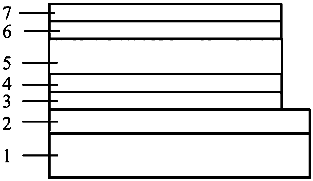
[0047] Clean the substrate composed of the substrate and the transparent conductive anode ITO, and dry it with nitrogen after cleaning; spin-coat PEDOT:PSS (1500rpm, 15nm) on the surface of the transparent conductive anode ITO to prepare the anode buffer layer, and the formed The film is baked (150°C, 30min); the electron blocking layer TAPC5nm is evaporated on the anode buffer layer, and the electron blocking layer is prepared by spin coating PVK:ZnO (60%:40%) ultraviolet photoactive layer (1500rpm, 120nm ), and baked (100° C., 15 min); a hole-blocking layer Bphen 5 nm was prepared by evaporation on the surface of the ultraviolet photoactive layer, and a metal cathode Ag (100 nm) was evaporated on the hole-blocking layer. Under standard test conditions: 350nm, 0.6mW / cm 2 Under the condition of -2V for ultraviolet light, the measured responsivity of the device is 1.5A / W.
Embodiment 2
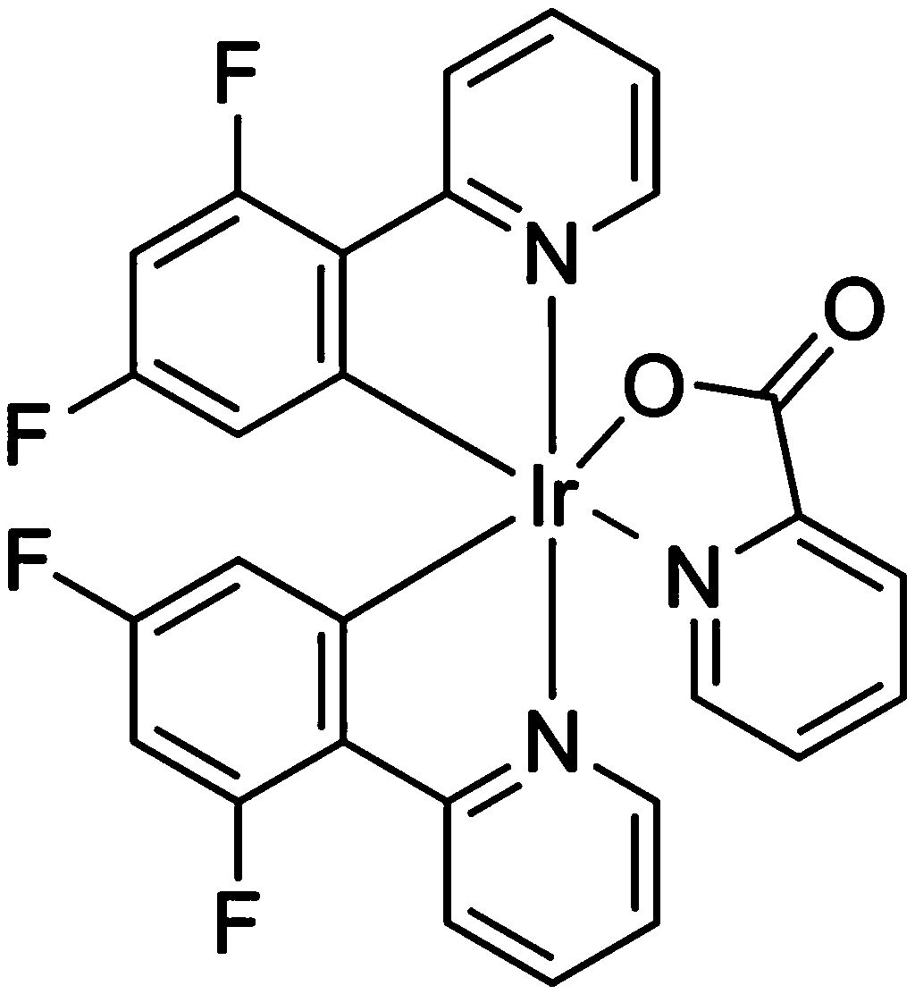
[0049] Clean the substrate composed of the substrate and the transparent conductive anode ITO, and dry it with nitrogen after cleaning; spin-coat PEDOT:PSS (1500rpm, 15nm) on the surface of the transparent conductive anode ITO to prepare the anode buffer layer, and the formed The film was baked (150°C, 30min); the electron blocking layer TAPC 5nm was evaporated on the anode buffer layer, and PVK:FIrpic:ZnO(60%:1%:39%) was prepared by spin coating on the electron blocking layer with ultraviolet light The active layer (1500rpm, 120nm) was baked (100°C, 15min); the hole blocking layer Bphen 5nm was prepared by evaporation on the surface of the ultraviolet photoactive layer, and the metal cathode Ag (100nm) was evaporated on the hole blocking layer. Under standard test conditions: 350nm, 0.6mW / cm 2 Under the condition of -2V for ultraviolet light, the measured responsivity of the device is 3.2A / W.
Embodiment 3
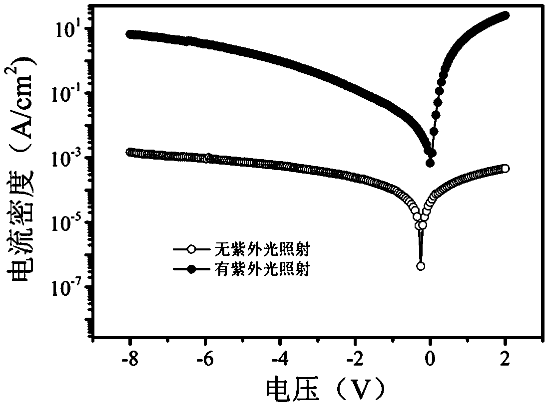
[0051] Clean the substrate composed of the substrate and the transparent conductive anode ITO, and dry it with nitrogen after cleaning; spin-coat PEDOT:PSS (1500rpm, 15nm) on the surface of the transparent conductive anode ITO to prepare the anode buffer layer, and the formed The film was baked (150°C, 30min); the electron blocking layer TAPC 5nm was evaporated on the anode buffer layer, and PVK:FIrpic:ZnO(60%:5%:35%) was prepared by spin coating on the electron blocking layer with ultraviolet light The active layer (1500rpm, 120nm) was baked (100°C, 15min); the hole blocking layer Bphen 5nm was prepared by evaporation on the surface of the ultraviolet photoactive layer, and the metal cathode Ag (100nm) was evaporated on the hole blocking layer. Under standard test conditions: 350nm, 0.6mW / cm 2 Under the condition of -2V for ultraviolet light, the measured responsivity of the device is 4.5A / W.
PUM
 Abstract
Description
Claims
Application Information


