Infrared night-vision goggle based on GeSn infrared detector

A technology of infrared detectors and night vision devices, applied in the field of microelectronics, can solve the problems of restricting the photosensitive efficiency, limiting the sensitivity and photosensitive efficiency of infrared night vision devices, and achieve the effects of improving photosensitive efficiency, expanding the absorption wavelength range, and low cost

Inactive Publication Date: 2016-04-20
XIDIAN UNIV
View PDF3 Cites 8 Cited by
  • Summary
  • Abstract
  • Description
  • Claims
  • Application Information

AI Technical Summary

Problems solved by technology

However, because Ge material is an indirect bandgap semiconductor material, it restricts the improvement of its

Method used


Image

  • Infrared night-vision goggle based on GeSn infrared detector
  • Infrared night-vision goggle based on GeSn infrared detector
  • Infrared night-vision goggle based on GeSn infrared detector

Examples


Embodiment 1

[0033] Embodiment 1: Fabrication of a GeSn infrared detector with a Sn composition of 0 and a Ge composition of 1 in the absorption zone.

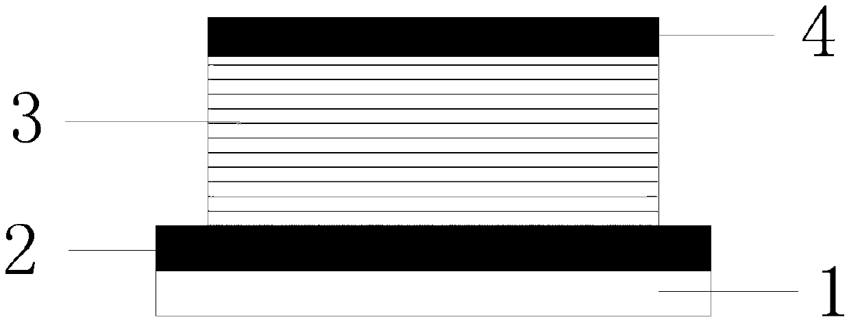
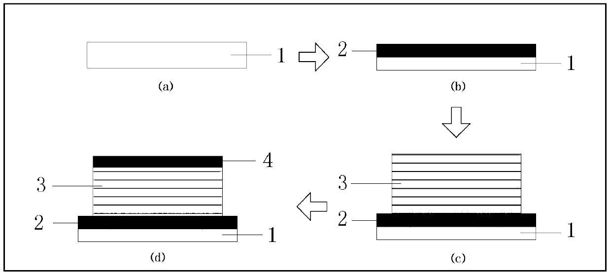
[0034] Step 1: Using ion implantation, the implantation dose in Si substrate 1 is 10 15 cm -2 , The phosphorus element with energy of 20KeV forms the N-type bottom electrode 2, such as image 3 b.

[0035] Step 2: Using molecular beam epitaxy process, on the bottom electrode 2, solid Ge and Sn are used as evaporation sources, and 10 -4 At the pressure of pa, the relaxed intrinsic GeSn single crystal is grown at 180℃, in which the Sn composition is 0 and the Ge composition is 1, forming an absorption zone 3, such as image 3 c.

[0036] Step 3: Using ion implantation, the implant dose is 10 in the top of GeSn material 15 cm -2 , Boron with an energy of 20KeV, form a P-type electrode 4 in the area where boron is implanted, such as image 3 d.

Embodiment 2

[0037] Embodiment 2: Fabrication of a GeSn infrared detector with a Sn composition of 0.10 and a Ge composition of 0.90 in the absorption zone.

[0038] Step 1: ion implantation to form the bottom electrode

[0039] The implant dose in Ge substrate 1 is 10 15 cm -2 , The phosphorus element with energy of 20KeV forms the N-type bottom electrode 2, such as image 3 b.

[0040] Step 2: Epitaxial relaxation of intrinsic GeSn single crystal

[0041] Using molecular beam epitaxy process, on the bottom electrode 2, solid Ge and Sn are used as evaporation sources, and 10 -4 The pressure of pa, at 180℃, the growth of a relaxed intrinsic GeSn single crystal, where the Sn composition is 0.10, and the Ge composition is 0.90, such as image 3 c.

[0042] Step 3: Ion implantation to form the upper electrode

[0043] Using ion implantation, the implant dose in the top of GeSn material is 10 15 cm -2 , Boron with an energy of 20KeV, forming a P-type electrode 4 in the area where boron is implanted, su...

Embodiment 3

[0044] Embodiment 3: Making a GeSn infrared detector with a Sn composition of 0.25 and a Ge composition of 0.75 in the absorption zone.

[0045] Step A: Using ion implantation, the implantation dose in the SOI substrate 1 is 10 15 cm -2 , The phosphorus element with energy of 20KeV forms the N-type bottom electrode 2, such as image 3 b.

[0046] Step B: Using the molecular beam epitaxy process, on the bottom electrode 2, solid Ge and Sn are used as evaporation sources, and 10 -4 The pressure of pa, at 180℃, the growth of a relaxed intrinsic GeSn single crystal, where the Sn composition is 0.25 and the Ge composition is 0.75, such as image 3 c.

[0047] Step C: Using ion implantation, the implant dose is 10 in the top of GeSn material 15 cm -2 , Boron with an energy of 20KeV, forming a P-type electrode 4 in the area where boron is implanted, such as image 3 d.


PUM


Abstract

The invention discloses an infrared night-vision goggle based on a GeSn infrared detector, and mainly aims to solve the problem that the existing infrared night-vision goggle is of low light sensing efficiency. The infrared night-vision goggle comprises an optical system, a detector, a signal processor and a display. The detector is a GeSn infrared detector, and comprises a substrate (1), a lower electrode (2), an absorption area (3) and an upper electrode (4), wherein the absorption area (3) is made of a GeSn material of which the general formula is Ge1-xSnx, x is a component of Sn, and 0<=x<=0.25. As the Sn element is added to the Ge element to form a relaxation intrinsic GeSn single crystal, the energy band structure of GeSn is changed from direct band gap to direct band gap while the forbidden bandwidth is decreased. Therefore, the light sensing frequency is increased, the red shift of the absorption edge is adjustable, and the light sensing efficiency and absorption wavelength range of the infrared night-vision goggle are improved.

Description

Technical field [0001] The invention belongs to the field of microelectronics technology, and particularly relates to an infrared night vision device, which can be used in meteorological, medical, national defense, and alarm systems. Background technique [0002] Infrared thermal imaging night vision device, also called passive infrared night vision device, mainly includes: optical system, detector, signal processor and display, such as figure 1 Shown. The optical system uses a conventional light gathering device, which is mainly used to process the infrared light emitted by the object to increase the intensity of the infrared; the detector converts the infrared light signal gathered by the optical system into an electrical signal to achieve infrared image shooting; signal processor , Including DSP processor and ARM processor, etc., used to repair and identify infrared images, convert digital signals into analog signals, and transmit them to the output; the display, preferably a ...

Claims


Application Information

Patent Timeline
IPC IPC(8): H01L31/101H01L31/028G02B23/12
CPCH01L31/101G02B23/12H01L31/028
Inventor 韩根全张春福周久人张进城郝跃
Owner XIDIAN UNIV
Why Eureka
Try Eureka