Production method for liquid crystal display panel

A technology of liquid crystal display panel and manufacturing method, which is applied in the direction of liquid crystal materials, chemical instruments and methods, instruments, etc., and can solve the problems of increasing panel cost, affecting panel quality, reducing process yield, etc.

Active Publication Date: 2016-04-27
TCL CHINA STAR OPTOELECTRONICS TECH CO LTD
View PDF7 Cites 17 Cited by
  • Summary
  • Abstract
  • Description
  • Claims
  • Application Information

AI Technical Summary

Problems solved by technology

Among them, the friction alignment type PI material forms an alignment film through the rubbing method (Rubbing). The rubbing method is to use flannelette rollers on the surface of the polymer PI film to perform contact-type directional mechanical friction. The energy provided by the rubbing polymer surface makes the high The main chain of the molecule is oriented due to extension, thereby controlling the interaction between the branch chain and the LC, so that the LC is arranged in the direction of the pre-tilt angle; therefore, it is easy to cause problems such as dust particles, static electricity residue, brush marks, etc. during friction alignment, which reduces the process yield.
The photo-alignment type PI material forms an alignment film through photo-alignment technology. The photo-alignment method uses the photochemical reaction of the ultraviolet photosensitive polymer monomer material to generate anisotropy, and the liquid crystal molecules interact with the branched chains on the surface of the alignment film. , in order to achieve a stable state with the smallest energy, the liquid crystal molecules are arranged along the direction of the largest force defined by the photo-alignment. The photo-alignment type PI material can solve the above problems, but due to the limited material properties, heat resistance and aging resistance The performance is not good, and the ability to anchor LC is also weak, which affects the quality of the panel
In addition, the PI material itself has high polarity and high water absorption, and it is easy to cause deterioration during storage and transportation, resulting in uneven phase matching, and the PI material is expensive, and the process of forming a film on TFT-LCD is also relatively complicated. lead to higher panel cost

Method used


Image

  • Production method for liquid crystal display panel
  • Production method for liquid crystal display panel
  • Production method for liquid crystal display panel

Examples


Embodiment Construction

[0039] In order to further illustrate the technical means adopted by the present invention and its effects, the following describes in detail in conjunction with preferred embodiments of the present invention and accompanying drawings.

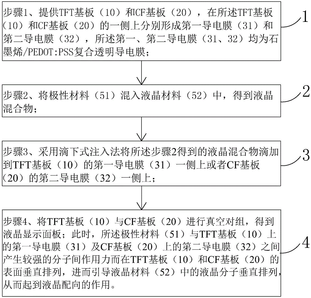
[0040] see figure 1 , the invention provides a method for manufacturing a liquid crystal display panel, comprising the following steps:

[0041] Step 1, providing a TFT substrate 10 and a CF substrate 20, forming a first conductive film 31 and a second conductive film 32 on one side of the TFT substrate 10 and the CF substrate 20 respectively, the first and second conductive films 31 , 32 are graphene / PEDOT:PSS composite transparent conductive film.

[0042] Specifically, the fabricated liquid crystal display panel is a multi-domain vertical alignment (Multi-domain Vertical Alignment, MVA) type liquid crystal display panel, and the TFT substrate 10 and CF substrate 20 provided in the step 2 are TFTs of a traditional MVA type liquid crystal di...


PUM


Abstract

The invention provides a production method for a liquid crystal display panel. According to the method, traditional ITO transparent conductive films on a TFT (thin film transistor) substrate and a CF (color filter) substrate are replaced with graphene / PEDOT:PSS composite transparent conductive films, polar materials are added to a liquid crystal mixture of the liquid crystal display panel, and a general structural formula of the polar materials is A-B; the head group A is mainly used for enabling larger intermolecular force to be generated between the polar materials and the graphene / PEDOT:PSS composite transparent conductive films; similar to a function of a PI branch chain, the tail group B is mainly used for enabling liquid crystal molecules to be arranged vertically in a steric hindrance manner and has a vertical alignment effect; that is, the polar materials can generate larger intermolecular force with the graphene / PEDOT:PSS composite transparent conductive films so as to be vertically arranged on the surface of the TFT substrate and the CF substrate, the liquid crystal molecules are guided to be arranged vertically, the polar materials are substituted for a PI alignment film to have a liquid crystal alignment effect, a PI alignment film preparation process is omitted, the production cost of the alignment film is reduced, and the capacity is improved.

Description

technical field [0001] The invention relates to the field of display technology, in particular to a method for manufacturing a liquid crystal display panel. Background technique [0002] Thin Film Transistor Liquid Crystal Display (TFT-LCD, Thin Film Transistor Liquid Crystal Display) has many advantages such as thin body, power saving, and no radiation, and has been widely used. Most of the TFT-LCDs currently on the market are backlight liquid crystal display devices, which include a liquid crystal display panel and a backlight module. The working principle of the liquid crystal display panel is to place liquid crystal molecules between two parallel glass substrates, and control the liquid crystal molecules to change direction through whether the glass substrates are energized or not, and refract the light from the backlight module to produce a picture. [0003] Usually, the liquid crystal display panel is composed of a color filter substrate (CF, ColorFilter), a thin film...

Claims


Application Information

Patent Timeline
Patent Type & Authority Applications(China)
IPC IPC(8): G02F1/1337G02F1/1343
CPCG02F1/133703G02F1/133707G02F1/13439C09K19/062C09K19/126C09K19/3444C08G2261/1424C08G2261/3223C08G2261/794C09K2019/122C09K2019/123C09K2019/3009C08G61/126C09K19/56H01L27/1292H01L27/124H01L27/1262C09D165/00C08L25/18C08K3/042G02F1/1343G02F1/133784H01L29/66742
Inventor 兰松李泳锐胡韬
Owner TCL CHINA STAR OPTOELECTRONICS TECH CO LTD
Why Eureka
Try Eureka