A polymer rectangular optical waveguide and microfluidic three-dimensional integrated chip and its preparation method
A three-dimensional integration, polymer technology, applied in the direction of optical waveguide, light guide, optics, etc., can solve the problems of complex process, easy blocking of channels and sensing windows, increase process cost, etc., to reduce bending loss and scattering loss, process Quick and flexible, simple process effect
- Summary
- Abstract
- Description
- Claims
- Application Information
AI Technical Summary
Problems solved by technology
Method used
Image
Examples
Embodiment 1
[0034] Example 1: Laser writing, wet etching to prepare SU-8-2005 waveguide, spin coating rotation speed 3000 rpm
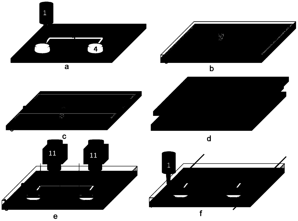
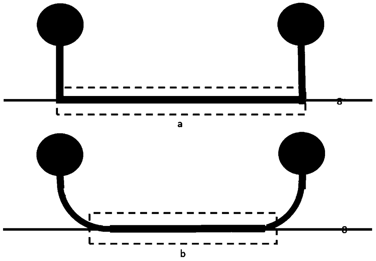
[0035] Use a carbon dioxide laser 1 to cut a surface-polished methyl methacrylate (PMMA) sheet with a thickness of 1mm (glass transition temperature 95°C), with a cutting power of 40W and a cutting speed of 50mm / s to cut out a rectangular methacrylic acid of 38cmx20cm Methyl ester microfluidic sheet substrate 2, use carbon dioxide laser 1 to write microfluidic channel 3 on methyl methacrylate microfluidic sheet substrate 2, laser energy 12W, cutting speed 15mm / s, realize Gaussian distribution groove (the width of the groove is 200 μm, the depth is 300 μm, the length of the middle segment of the three-segment structure is 1.5 cm, parallel to the long side of the rectangular sample (the center of the line segment is located on the vertical line of the long side), the distance between the nearest long side is 5 mm, and the line segment The end point of the middle li...
Embodiment 2
[0041] Example 2: Nanoimprinting, wet etching of SU-8-100 waveguide, spin coating at 6000 rpm
[0042] A surface-polished methyl methacrylate substrate sheet (glass transition temperature 95°C) with a thickness of 1mm was cut with a carbon dioxide laser 1, the cutting power was 40W, and the cutting speed was 50mm / s, and a rectangular substrate of 40cmx20cm was cut. Thermal embossing is performed on the methyl methacrylate microfluidic sheet substrate 2. The size of the Si template is the same as 40cmx20cm. There is a strip-shaped structure of protrusions on the Si template. The protrusions are 40 μm high and 40 μm wide. The protrusion pattern is a three-stage structure. The length of the middle line segment of the structure is 1.5cm, parallel to the long side of the rectangular sample (the center of the line segment is located on the vertical line of the long side), the distance between the nearest long side is 5mm, the endpoints of the middle line segment are connected vertica...
Embodiment 3
[0048] Example 3: Nanoimprinting, wet etching to prepare SU-8-2005 waveguide, spin-coating at 4000 rpm
[0049] A surface-polished methyl methacrylate substrate sheet (glass transition temperature 95°C) with a thickness of 1mm was cut with a carbon dioxide laser 1, the cutting power was 40W, and the cutting speed was 50mm / s, and a rectangular substrate of 40cmx20cm was cut. Thermal embossing is performed on the methyl methacrylate microfluidic sheet substrate 2. The size of the Si template is the same as 40cmx20cm. There is a strip-shaped structure of protrusions on the Si template. The protrusions are 5 μm high and 5 μm wide. The protrusion pattern is a three-stage structure. The length of the middle line segment of the structure is 1.5cm, parallel to the long side of the rectangular sample (the center of the line segment is located on the vertical line of the long side), the distance between the nearest long side is 5mm, and the end point of the middle line segment is 1 / 4 of ...
PUM
 Abstract
Description
Claims
Application Information


