

Preparation method and application of Cu2ZnSnS4/graphene composite semiconductor film
A graphene composite, graphene film technology, applied in semiconductor devices, electrolytic capacitors, coatings and other directions, can solve the problems of low solar energy utilization, easy recombination of photogenerated electrons and holes, affecting light absorption efficiency, etc. Industrialized production, low cost, cost reduction effect
- Summary
- Abstract
- Description
- Claims
- Application Information
AI Technical Summary
Problems solved by technology
Method used
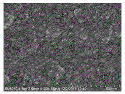
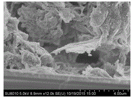
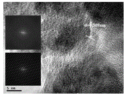
Image

Examples
Embodiment 1
[0028] a Cu 2 ZnSnS 4 The preparation method of / graphene composite semiconductor thin film comprises the following steps:
[0029] (1) Cleaning of FTO conductive glass substrate: SnO doped with F 2 Put the transparent conductive glass FTO into acetone, absolute ethanol and deionized water in turn for ultrasonic cleaning for 10 minutes, and then dry;
[0030] (2) Preparation of graphene film skeleton: add 0.01 g of redox graphene powder prepared by improved hummer method to 50 ml of ethylene glycol solution, disperse it ultrasonically for 10 min with an ultrasonic pulverizer, and then use a dropper to absorb 0.02 ml of graphene suspension , added dropwise on the conductive surface of FTO glass, placed in a blower dryer, and dried at a constant temperature of 60°C to obtain a graphene film;
[0031] (3) Preparation of chemical reaction precursor solution: add 4mmol copper chloride, 2mmol zinc chloride, 2mmol stannous chloride to 50ml of ethylene glycol in turn, stir until ful...
Embodiment 2
[0034] a Cu 2 ZnSnS 4 The preparation method of / graphene composite semiconductor thin film comprises the following steps:
[0035] (1) Cleaning of FTO conductive glass substrate: SnO doped with F 2 Put the transparent conductive glass FTO into acetone, absolute ethanol and deionized water in turn for ultrasonic cleaning for 10 minutes, and then dry;
[0036] (2) Preparation of graphene film skeleton: add 0.1 g of redox graphene powder prepared by improved hummer method to 50 ml of ethylene glycol solution, disperse it ultrasonically for 10 min with an ultrasonic pulverizer, and then use a dropper to absorb 0.1 ml of graphene suspension , dropped on the conductive surface of FTO glass, placed in a blower dryer, and dried at a constant temperature of 200°C to obtain a graphene film;
[0037] (3) Preparation of chemical reaction precursor solution: Add 4mmol copper chloride, 2mmol zinc chloride, 2mmol stannous chloride to 50ml of ethylene glycol in turn, stir until fully disso...
Embodiment 3
[0040] a Cu 2 ZnSnS 4 The preparation method of / graphene composite semiconductor thin film comprises the following steps:
[0041] (1) Cleaning of FTO conductive glass substrate: SnO doped with F 2 Put the transparent conductive glass FTO into acetone, absolute ethanol and deionized water in turn for ultrasonic cleaning for 10 minutes, and then dry;
[0042] (2) Preparation of graphene film skeleton: add 0.05g of redox graphene powder prepared by improved hummer method to 50ml of ethylene glycol solution, ultrasonically disperse for 10min with an ultrasonic pulverizer, and then use a dropper to absorb 0.06ml of graphene suspension , added dropwise on the conductive surface of FTO glass, placed in a blower dryer, and dried at a constant temperature of 100°C to obtain a graphene film;
[0043] (3) Preparation of chemical reaction precursor solution: add 4mmol copper chloride, 2mmol zinc chloride, 2mmol stannous chloride to 50ml of ethylene glycol in turn, stir until fully dis...
PUM
| Property | Measurement | Unit |
|---|---|---|
| specific surface area | aaaaa | aaaaa |
| breaking strength | aaaaa | aaaaa |
| transmittivity | aaaaa | aaaaa |
Abstract
Description
Claims
Application Information