Oxide-metal multilayer film back contact crystalline silicon solar cell and preparation method thereof

A technology for solar cells and oxide films, applied in the field of solar cells, can solve the problems of raw material silane being inflammable and explosive, reducing the photo-generated current of cells, low filling factor, etc., and achieving the effects of low cost, reduced compounding, and simple equipment

Active Publication Date: 2016-07-20
江苏润阳悦达光伏科技有限公司
View PDF6 Cites 14 Cited by
  • Summary
  • Abstract
  • Description
  • Claims
  • Application Information

AI Technical Summary

Problems solved by technology

However, IBC-SHJ solar cells currently have the following problems: 1. The equipment is expensive, and the raw material silane is a flammable and explosive chemical
3. It is necessary to use transparent conductive films such as ITO and low-temperature silver paste, which are expensive and difficult to mass produce
However, the front-junction oxide-metal multilayer film / silicon-based solar cell has the following disadvantages: (1) The emitter of the cell contains a layer of metal film, which will greatly reduce the efficiency of the cell due to the reflection and absorption of light by the metal film. Photogenerated current; (2) The metal electrode on the front surface and the emitter are only partially in contact (~8%), the series resistance is large, and the fill factor is low

Method used


Image

  • Oxide-metal multilayer film back contact crystalline silicon solar cell and preparation method thereof
  • Oxide-metal multilayer film back contact crystalline silicon solar cell and preparation method thereof
  • Oxide-metal multilayer film back contact crystalline silicon solar cell and preparation method thereof

Examples


Embodiment 1

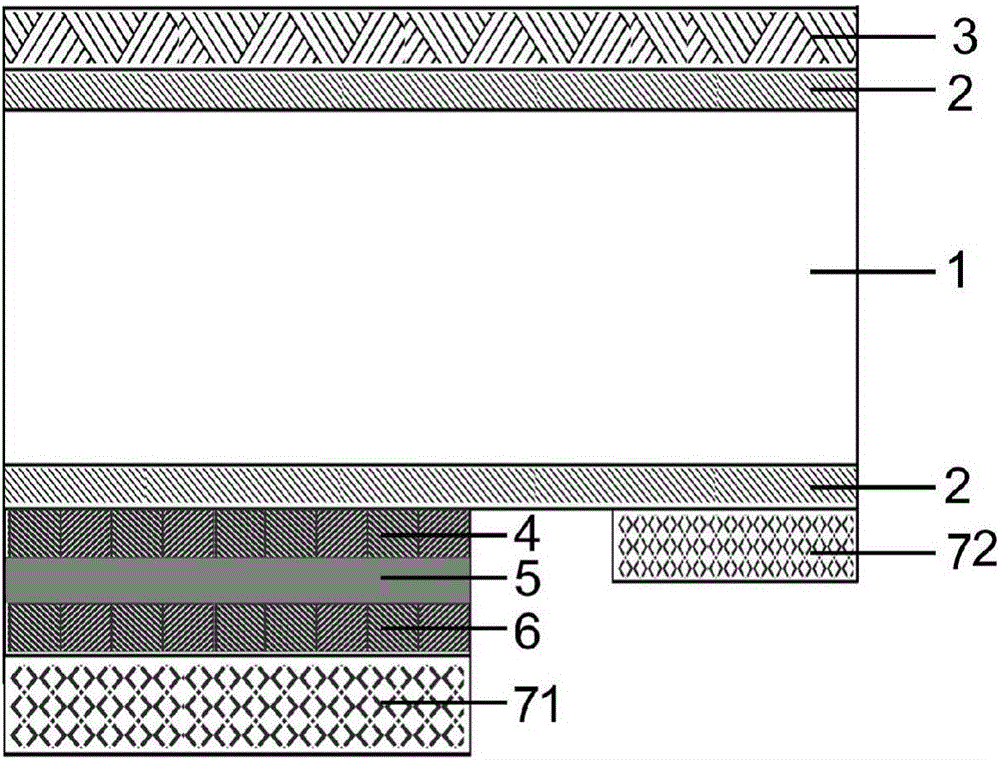
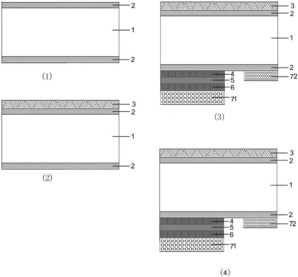
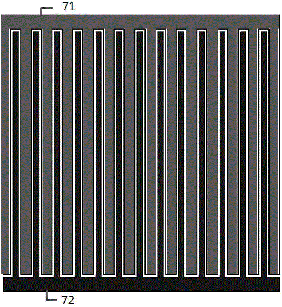
[0041] Such as figure 1 As shown in , the structure provided in this embodiment is an oxide-metal multilayer film back-contact crystalline silicon solar cell, including a crystalline silicon wafer 1, and a passivation layer 2 is provided on the front surface and the back surface of the crystalline silicon wafer 1. An emitter, an emitter metal electrode 71 and a base metal electrode 72 are arranged on the layer 2, and the emitter is composed of a first oxide film 4, a metal film 5 and a second oxide film 6; wherein the first oxide film 4 or for WO 3 film, the metal film is Ag film, and the second oxide film 6 is V 2 o 5 film.

[0042] The thickness of the first oxide film 4 is 5-30 nm, the thickness of the metal film 5 is 2-20 nm, and the thickness of the second oxide film 6 is 5-80 nm.

[0043] An antireflection film 3 is provided on the passivation layer 2 of the front surface of the crystalline silicon wafer 1 .

[0044] There is a gap between the emitter metal electrod...

Embodiment 2

[0053] The structure provided in this embodiment is an oxide-metal multilayer film back-contact crystalline silicon solar cell. The difference from Embodiment 1 is that the passivation layer 2 is Al 2 o 3 passivation layer, the first oxide film 4 is V 2 o 5 , the metal film 5 is an Au film, and the second oxide film 6 is a WO 3 .

[0054] The above structure is an oxide-metal multilayer film back-contact crystalline silicon solar cell, which is prepared by the following method:

[0055] (1) The n-type or p-type single crystal silicon wafer is cleaned by RCA process, and then a layer of Al is deposited on the front and rear surfaces of the silicon wafer by atomic layer deposition (ALD) technology. 2 o 3 Passivation layer, set the deposition temperature to 200°C, Al(TMA), N 2 、H 2 The pulse time of O is: 0.1s, 10s and 0.1s, the flow rates are: 150sccm, 150sccm and 200sccm, respectively, and 10-30 cycles are performed to deposit 1-3nm Al on the surface of the silicon wafer...

Embodiment 3

[0062] The structure provided in this embodiment is an oxide-metal multilayer film back-contact crystalline silicon solar cell. The difference from Embodiment 1 is that the passivation layer 2 is TiO 2 passivation layer, the first oxide film 4 is V 2 o 5 , the metal film 5 is a Pd film, and the second oxide film 6 is NiO.

[0063] The above structure is an oxide-metal multilayer film back-contact crystalline silicon solar cell, which is prepared by the following method:

[0064] (1) Clean the n-type or p-type single crystal silicon wafer with the RCA process, and then deposit a layer of TiO on the front and rear surfaces of the silicon wafer using atomic layer deposition (ALD) technology 2 Passivation layer, set the deposition temperature to 200-300°C, TiCl 4 , N 2 、H 2 The pulse time of O is: 1s, 3s and 1s respectively, the flow rate is respectively: 150sccm, 150sccm and 200sccm, carry out 10~30 cycles, deposit the titanium dioxide of 1~3nm on the silicon chip surface; ...


PUM

PropertyMeasurementUnit
thicknessaaaaaaaaaa
thicknessaaaaaaaaaa
thicknessaaaaaaaaaa

Abstract

The invention discloses an oxide-metal multilayer film back contact crystalline silicon solar cell, which comprises a crystalline silicon wafer, wherein passivation layers are arranged on the front surface and the back surface of the crystalline silicon wafer; the passivation layer on the back surface is provided with an emitter, an emitter metal electrode and a base metal electrode; the emitter comprises a first oxide thin film, a metal film and a second oxide thin film; the first oxide thin film or the second oxide thin film is a WO3 thin film, an NiO thin film or a V2O5 thin film; and the metal thin film is an Ag thin film, an Au thin film, a Pd thin film, a Cu thin film, an Ni thin film, an Mo thin film, a W thin film or an Al thin film. The surface of the cell is not shielded by a metal grid line; the raw materials do not include inflammable, explosive or toxic materials and are friendly to environment; expensive devices of a photoetching device, a laser device and the like and a complicated technological process are not needed in the overall preparation process; and the crystalline silicon solar cell disclosed by the invention is free of a high temperature, simple in processing step and suitable for large-scale production, does not need to use a transparent conductive thin film, is low in cost and has a wide application prospect.

Description

technical field [0001] The invention belongs to the technical field of solar cells, and in particular relates to an oxide-metal multilayer film back-contact crystalline silicon solar cell and a preparation method thereof. Background technique [0002] The most common structure type of solar cells is the p-n junction type of inorganic material system, which can be divided into homojunction and heterojunction according to the similarities and differences of materials. Heterojunction solar cells can avoid the high-temperature diffusion process, and prepare thin films and silicon substrates at low temperatures to form p-n junctions. The current commercial silicon-based heterojunction solar cells mainly include a-Si:H / c-Si heterojunction with intrinsic thin layer (HIT) and interdigitated backcontact silicon heterojunction (IBC-SHJ) solar cells. . [0003] The front surface of the IBC-SHJ solar cell uses a larger band of semiconductor material as an anti-reflection film and pass...

Claims


Application Information

Patent Timeline
Patent Type & Authority Applications(China)
IPC IPC(8): H01L31/0224H01L31/0216H01L31/18
CPCH01L31/02167H01L31/02245H01L31/1868Y02E10/50Y02P70/50
Inventor 沈辉包杰吴伟梁刘宗涛
Owner 江苏润阳悦达光伏科技有限公司
Why Eureka
Try Eureka