Method for making transparent conductive layer for improving brightness of light-emitting diode chip

A technology of light-emitting diodes and transparent conductive layers, applied in circuits, electrical components, semiconductor devices, etc., can solve the problem that light cannot be used to improve light efficiency, and achieve the effect of increasing the output rate and improving luminous efficiency

Active Publication Date: 2018-10-26
XIANGNENG HUALEI OPTOELECTRONICS
View PDF3 Cites 0 Cited by
  • Summary
  • Abstract
  • Description
  • Claims
  • Application Information

AI Technical Summary

Problems solved by technology

[0006] In view of this, the present invention provides a method for manufacturing a transparent conductive layer that improves the brightness of light-emitting diode chips, which solves the disadvantage that the internal loss of light in traditional LED chips cannot be used to improve light efficiency.

Method used


Image

  • Method for making transparent conductive layer for improving brightness of light-emitting diode chip
  • Method for making transparent conductive layer for improving brightness of light-emitting diode chip
  • Method for making transparent conductive layer for improving brightness of light-emitting diode chip

Examples


Embodiment 1

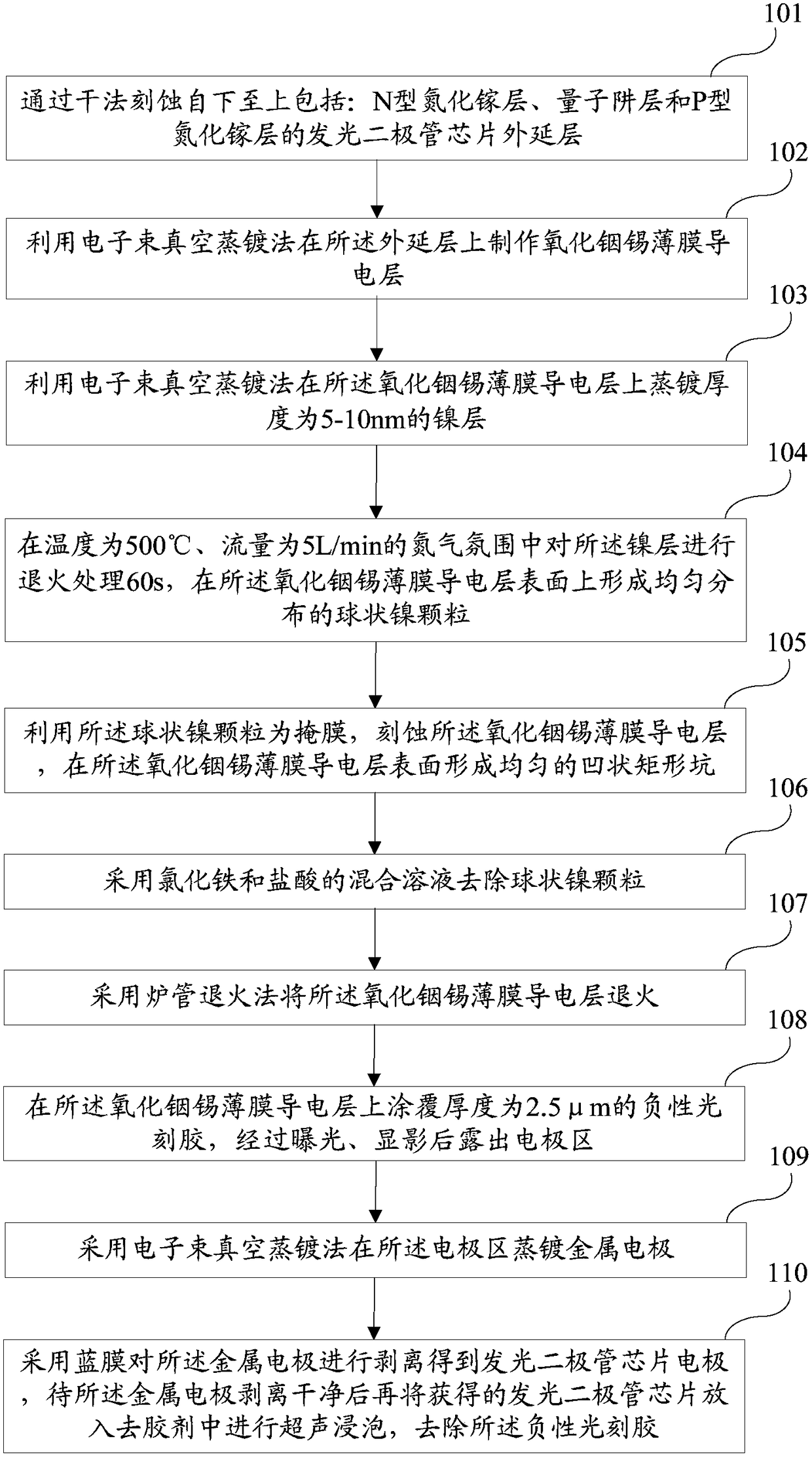
[0057] Such as figure 1 As shown in FIG. 2 , it is a schematic flowchart of an alternative embodiment of the method for manufacturing a transparent conductive layer for improving the brightness of a light-emitting diode chip according to the present invention. In the present invention, the surface of the ITO film layer of the light-emitting diode chip is made into a nano-scale concavo-convex shape, which is beneficial to the light emission inside the light-emitting diode chip, thereby improving the luminous efficiency of the light-emitting diode chip. The manufacturing method of the transparent conductive layer for improving the brightness of the light-emitting diode chip described in this embodiment includes the following steps:

[0058] Step 101, dry etching the epitaxial layer of the light emitting diode chip including: N-type GaN layer, quantum well layer and P-type GaN layer from bottom to top.

[0059] Step 102, using an electron beam vacuum evaporation method to form a...

Embodiment 2

[0072] Such as Figure 7 as shown, Figure 7 It is a schematic flowchart of the method for manufacturing a transparent conductive layer for improving the brightness of a light-emitting diode chip described in Embodiment 2 of the present invention. In this embodiment, a specific method for making the concave-convex structure on the surface of the ITO layer is provided. The manufacturing method of the transparent conductive layer for improving the brightness of the light-emitting diode chip in this embodiment includes the following steps:

[0073] Step 701, dry etching the epitaxial layer of the LED chip including: N-type GaN layer, quantum well layer and P-type GaN layer from bottom to top.

[0074] Preferably, in this step, the N-type gallium nitride layer, the quantum well layer and the epitaxial layer of the P-type gallium nitride layer of the light-emitting diode chip are formed from bottom to top with an etching depth of 1 μm and a width of the scribe line between 8-14 μ...

Embodiment 3

[0091] Such as Figure 8 As shown, it is a schematic flowchart of a specific embodiment of the manufacturing method of the transparent conductive layer for improving the brightness of the light-emitting diode chip disclosed in this embodiment. The manufacturing method of the transparent conductive layer for improving the brightness of the light-emitting diode chip in this embodiment includes the following steps:

[0092]Step 801, dry etching the epitaxial layer of the N-type GaN layer, the quantum well layer and the P-type GaN layer of the light-emitting diode chip with an etching depth of 1 μm and a dicing line width of 10 μm from bottom to top, forming step and expose the N-type gallium nitride layer.

[0093] Step 802, under the conditions of a chamber temperature of 160°C, an oxygen flow rate of 10 sccm, and a vacuum degree of 3×10⁻⁵ Torr, an indium tin oxide thin film conductive layer is formed on the epitaxial layer by electron beam vacuum evaporation, wherein the The ...


PUM

PropertyMeasurementUnit
thicknessaaaaaaaaaa
thicknessaaaaaaaaaa

Abstract

The invention discloses a transparent conducting layer manufacturing method for increasing light emitting diode chip brightness. The method comprises following steps: etching a light emitting diode chip epitaxial layer through a dry method preparing a tin indium oxide film conducting layer on the epitaxial layer; preparing a nickel layer with thickness from 5 to 10 nm on the tin indium oxide film conducting layer by a vapor plating method; performing annealing to the nickel layer; forming uniformly distributed spherical nickel particles on the tin indium oxide film conducting layer surface; etching the tin indium oxide film conducting layer with the spherical nickel particles as a mask layer to form uniform concave rectangular pits on the tin indium oxide film conducting layer surface; removing the spherical nickel particles; coating the tin indium oxide film conducting layer with negative photoresist and exposing electrode zones after exposure and development; preparing metal electrodes at the electrode zones by means of the vacuum electron beam evaporation method; peeling the metal electrodes to obtain light emitting diode chip electrodes and removing the negative photoresist. By means of the method, the brightness of light diode chip is increased.

Description

technical field [0001] The invention relates to the technical field of semiconductor chip fabrication, and more specifically, to a method for fabricating a transparent conductive layer for improving the brightness of a light-emitting diode chip. Background technique [0002] Light-emitting diode (Light-Emitting Diode, referred to as LED) is a semiconductor electronic device that converts electrical energy into light energy. ), the working current is very small (some can emit light with only a few tenths of milliamperes), the impact resistance and shock resistance are good, the reliability is high, the service life is long, and the characteristics of easily modulating the intensity of light emission are very popular. [0003] With the vigorous development of the third-generation semiconductor technology, semiconductor lighting has become the focus of social development due to its advantages of energy saving, environmental protection, high brightness, and long life. GaN (gall...

Claims


Application Information

Patent Timeline
Patent Type & Authority Patents(China)
IPC IPC(8): H01L33/42
CPCH01L33/42H01L2933/0016
Inventor 李胤强徐平
Owner XIANGNENG HUALEI OPTOELECTRONICS
Why Eureka
Try Eureka