Ultrasonic-bonded micro-fluidic chip and preparation method thereof

A microfluidic chip and ultrasonic technology, which is applied in the field of biological science micro-total analysis systems, can solve the problems of difficult cleaning, collapse of chip microchannels, and unfavorable mass production.

Inactive Publication Date: 2016-08-10
北京同方华光系统工程有限公司
View PDF4 Cites 12 Cited by
  • Summary
  • Abstract
  • Description
  • Claims
  • Application Information

AI Technical Summary

Problems solved by technology

However, during the thermal pressing process, the polymer chip is deformed by the coupling effect of heat and pressure, which will cause the chip to collapse in the microfluidic channel, thereby affecting the bonding effect of the microfluidic chip, and in the direct thermal bonding process, the heating And the pressure holding process takes a long time, which is not conducive to mass production. In addition, after thermocompression bonding, the organic matter on the microfluidic chip will adhere to the heating block or gasket, which is not easy to clean

Method used


Image

  • Ultrasonic-bonded micro-fluidic chip and preparation method thereof
  • Ultrasonic-bonded micro-fluidic chip and preparation method thereof
  • Ultrasonic-bonded micro-fluidic chip and preparation method thereof

Examples


Embodiment 1

[0027] figure 1 The flow chart of the method for preparing an ultrasonically bonded microfluidic chip provided in Example 1 of the present invention, as shown in figure 1 As shown, the method includes:

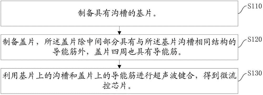
[0028] S110, preparing a substrate with grooves.

[0029] Specifically, design the characteristic size and structure of the required substrate, and use the photolithography mask technology to manufacture the corresponding substrate, that is, make the photolithography master mold with the required groove through SU-8 photoresist photolithography, After a layer of conductive layer is sputtered by magnetron, the nickel brief injection mold is made by electroforming process, and finally the substrate is injected by a disc injection molding machine.

[0030] Specifically, the material of the substrate is a thermoplastic polymer. For example, polymethylmethacrylate (polymethylmethacrylate, PMMA), polycarbonate (Polycarbonate, PC), cycloolefin polymer (Cyclo-olefin polymer, COP) a...

Embodiment 2

[0042] A method for preparing a PMMA ultrasonically bonded microfluidic chip, the steps are as follows:

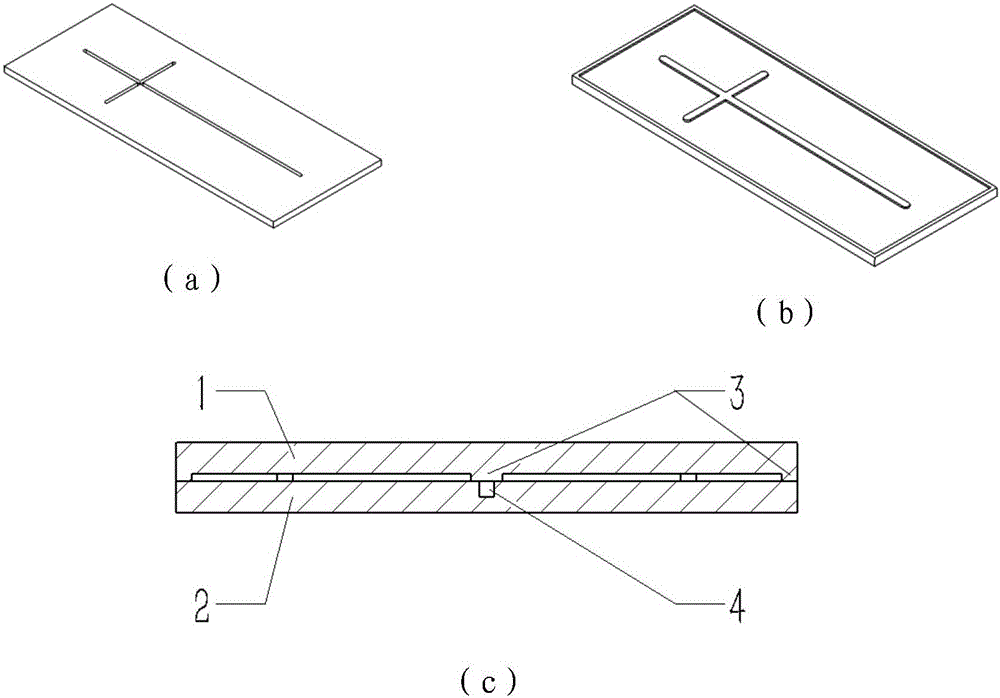
[0043] 1. The specification of the PMMA substrate is 37.5*25*0.6mm, and the substrate with cross-shaped grooves is produced by using photolithography mask technology, such as figure 2 (a) shown. Wherein, the groove width and depth are both 100 μm.

[0044] 2. The specification of the PMMA cover sheet is 37.5*25*0.6mm. The photolithographic mask technology is used to make the cover sheet with cross-shaped energy directors, such as figure 2 (b) shown. The cross-shaped energy director and figure 2 Corresponding to the position of the cross-shaped groove in (a), the width of the cross-shaped energy director is 200 μm, and the thickness is 50 μm. In addition, there are also energy-directing ribs around the cover sheet, and the width of the energy-directing ribs around the cover sheet is 100 μm.

[0045] 3. Fix the substrate and cover sheet with fixtures, align the groov...

Embodiment 3

[0047] A method for preparing a PC ultrasonically bonded microfluidic chip, the steps are as follows:

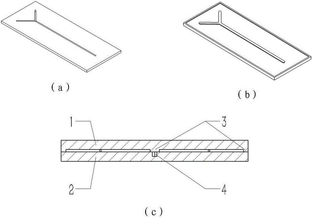
[0048] 1. The specification of the PC substrate is 45*37*0.6mm, and the substrate with Y-shaped grooves is produced by photolithography mask technology, such as image 3 (a) shown. Wherein, the groove width and depth are both 150 μm.

[0049] 2. The specification of the PC cover sheet is 45*37*0.6mm, and the photolithography mask technology is used to make the cover sheet with Y-shaped energy guiding ribs, such as image 3 (b) shown. The Y-shaped energy director and image 3 Corresponding to the position of the Y-shaped groove in (a), the cross-shaped energy director has a width of 250um and a thickness of 50μm. In addition, there are also energy-directing ribs around the cover sheet, and the width of the energy-directing ribs around the cover sheet is 100 μm.

[0050] 3. Fix the substrate and cover sheet with fixtures, align the grooves on the substrate with the energy...


PUM


Abstract

The invention relates to an ultrasonic-bonded micro-fluidic chip and a preparation method thereof. The preparation method comprises the following steps: preparing a substrate with a groove; preparing a cover glass plate, wherein the periphery and the central part of cover glass plate are provided with energy guiding ribs of a same structure with the groove of the substrate; and carrying out ultrasonic bonding in virtue of the groove on the substrate and the energy guiding ribs on the cover glass plate so as to obtain the micro-fluidic chip. According to the invention, a targeted cover glass plate structure is designed on the basis of the characteristic size of the substrate, so a making process for a chip injection mould is greatly simplified and production efficiency is improved; mediums like an adhesive are not needed in the process of packaging, so pollution is not produced; connection surfaces are in fusion connection, so bonding strength is high; moreover, before ultrasonic bonding, pre-treatment is not needed, so preparation time is shortened, bonding time in the aspect of bonding technological parameters is reduced, a packaging speed is fast, continuous automatic production can be realized, and thus, large-scale production of the polymer chip is realized.

Description

technical field [0001] The invention relates to the technical field of micro total analysis system (micro total analysis system, μ-TAS) in biological sciences, in particular to an ultrasonic bonding microfluidic chip and a preparation method thereof. Background technique [0002] Microfluidic chips are currently a hot field in the development of micro-total analysis systems. Its goal is to miniaturize and integrate laboratory functions in the fields of biology, chemistry, medicine, etc. into a small chip, which can simultaneously analyze hundreds of samples in a few minutes or even less, and can realize the sample online. The whole process of pretreatment and analysis is used to realize various functions of routine laboratories. [0003] In the manufacture of microfluidic devices, polymers have gradually replaced glass, quartz, silicon and other materials. Microfluidic devices made of polymers have the advantages of light weight, small size, corrosion resistance, good insul...

Claims


Application Information

Patent Timeline
Patent Type & Authority Applications(China)
IPC IPC(8): B01L3/00
CPCB01L3/502707B01L2300/0809B01L2300/0854
Inventor 刘祝凯胡在兵郭哲许斌刘伟
Owner 北京同方华光系统工程有限公司
Why Eureka
Try Eureka