Doping silylene based MEMS piezoresistive pressure sensor and manufacturing method thereof

A pressure sensor, piezoresistive technology, applied in the measurement of fluid pressure by changing ohmic resistance, and the measurement of the property force of piezoresistive materials. problems such as limited sensitivity, to achieve the effect of good compatibility, high sensitivity, and simple manufacturing process

Active Publication Date: 2016-08-10
HUAZHONG UNIV OF SCI & TECH
View PDF7 Cites 12 Cited by
  • Summary
  • Abstract
  • Description
  • Claims
  • Application Information

AI Technical Summary

Problems solved by technology

[0005] The MEMS piezoresistive pressure sensor based on doped silicene provided by the present invention solves the problems of large phase volume, limited reliability and sensitivity of traditional pressure sensors and the incompatibility of graphene pressure sensors with current silicon-based semiconductor processes

Method used


Image

  • Doping silylene based MEMS piezoresistive pressure sensor and manufacturing method thereof
  • Doping silylene based MEMS piezoresistive pressure sensor and manufacturing method thereof
  • Doping silylene based MEMS piezoresistive pressure sensor and manufacturing method thereof

Examples


no. 1 example

[0043] A manufacturing method of the first embodiment of the present invention comprises the following steps:

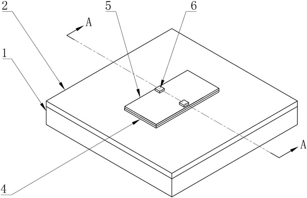
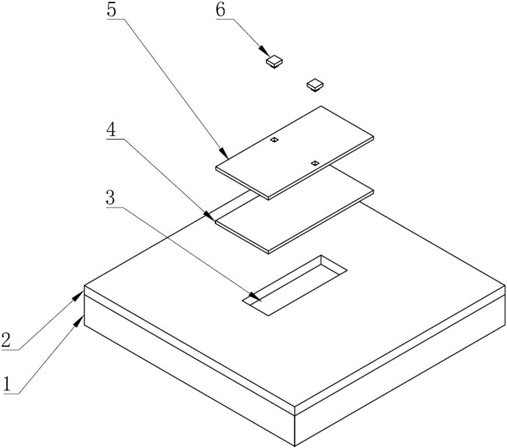
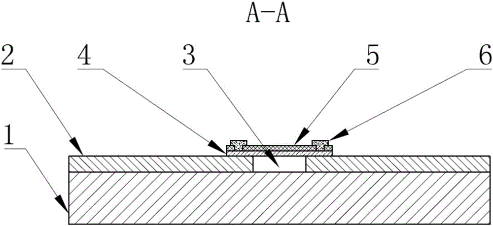
[0044] (1) After cleaning and drying a 300 μm thick silicon wafer as the substrate 1, deposit SiO with a thickness of 300 nm on its surface 2 insulating layer 2, and then cutting the silicon wafer into square pieces of 12mm×12mm;

[0045] (2) Reaction-coupled plasma (ICP) etching is performed on the insulating layer 2 to form a rectangular cavity 3, the depth of the cavity 3 is equal to the thickness of the insulating layer 2;

[0046] (3) Carry out sputter cleaning to Ag plate (cleaning condition is 600eV, Ar + ion, 10 -2 mT), annealed at 400°C to form a sharp P(1╳1), in ultra-high vacuum 10 -9 Epitaxial deposition of silicene at mT and substrate temperature of 250°C to form Ag-silicene layer;

[0047] (4) Invert the Ag-silicene layer so that the silicene faces down, and transfer the silicene face to the cavity 3 containing SiO 2 On the substrate 1 of the insulat...

no. 2 example

[0055] The manufacturing method of the second embodiment includes the following steps:

[0056] (1) Wash and dry a 300 μm thick wafer silicon (111) sheet as substrate 1, and deposit a layer of 1 μm thick β-Si on the upper surface 3 N 4 (0001) as insulating layer 2;

[0057] (2) Perform photolithography on the lower surface of the wafer silicon (111), and use ICP etching to obtain the cavity 3;

[0058] (3) In β-Si 3 N 4 (0001) surface carries out MBE deposition silicene thin film 4, and on described silicene thin film 4, forms a layer of 10nm thick SiO with LPCVD deposition 2 An anti-oxidation protective layer 5, followed by doping the silicene film 4;

[0059] (4) In the SiO 2 The surface of the anti-oxidation protection layer 5 corresponds to the position of the cavity 3, and two metal electrode patterns are obtained by photolithography, and 20 nm of Ti and 200 nm of Au are successively deposited on the two metal electrode patterns to form two metal electrodes 6 , the...


PUM

PropertyMeasurementUnit
thicknessaaaaaaaaaa
thicknessaaaaaaaaaa
thicknessaaaaaaaaaa

Abstract

The invention discloses a doping silylene based MEMS piezoresistive pressure sensor and a manufacturing method thereof. According to one method, an insulating layer is deposited at the surface of a substrate based on a surface silicon processing technology, and the insulating layer is etched so as to form a cavity; silylene is deposited on Ag, and the cavity is completely covered; the Ag substrate is peeled off, and then anti-oxidation protection and doping are carried out on a silylene film; and finally, two metal electrodes are deposited at the edge above the film, and each electrode is welded with a wire. According to another method, a mode of a traditional piezoresistive pressure sensor is adopted, wherein the traditional piezoresistive pressure sensor comprises glass, a substrate, an insulating layer, a silylene film, an anti-oxidation protection layer and metal electrodes from the bottom up. The doping silylene based MEMS piezoresistive pressure sensor has the advantages of good compatibility between silylene and the traditional semiconductor technology, simple manufacturing process, higher sensitivity and wider application.

Description

technical field [0001] The invention belongs to the field of microelectromechanical systems (MEMS) pressure detection devices, and in particular relates to a MEMS piezoresistive pressure sensor based on doped silicene and a manufacturing method thereof. Background technique [0002] With the rise of wearable devices, micro-nano pressure sensors with small size and high sensitivity are required in the fields of nano-biochemistry and nano-medicine, such as injection needle-type piezoresistive pressure sensors and can measure cardiovascular, intracranial, urethra, uterus and intraocular pressure sensors. pressure sensor. The development trend of pressure sensors is smaller size, from micrometer scale to nanometer scale, higher sensitivity, higher reliability, and wider application range, so as to adapt to some special occasions such as the measurement of internal blood pressure or tissue pressure. [0003] The basic process of the existing traditional MEMS silicon pressure sen...

Claims


Application Information

Patent Timeline
Patent Type & Authority Applications(China)
IPC IPC(8): G01L1/18G01L9/06
CPCG01L1/18G01L9/06
Inventor 汪学方占善男
Owner HUAZHONG UNIV OF SCI & TECH
Why Eureka
Try Eureka