Device and method for parallel mask-less scanning micro-nano processing based on atmospheric pressure plasma jet tube

A micro-nano processing, plasma technology, applied in the fields of nanotechnology, nanotechnology, nanotechnology for materials and surface science, can solve the problem that it is not suitable for scanning processing, and the processing resolution cannot be further improved to submicron and nanometer quantities. high-efficiency maskless etching effect

Active Publication Date: 2016-08-24
UNIV OF SCI & TECH OF CHINA
View PDF4 Cites 14 Cited by
  • Summary
  • Abstract
  • Description
  • Claims
  • Application Information

AI Technical Summary

Problems solved by technology

Ryutaro Shimane et al. used microfabrication technology to process 2 μm diameter cylindrical microhole nozzle arrays and exhaust grooves on silicon wafers, adsorbed pollen particles at the nozzle openings, and used the light irradiation effect generated by plasma to realize the protection of pollen particles. Surface modification, but this method cannot lead to plasma microjet flow, and the processed sample must be in contact with the nozzle, which is not suitable for scanning processing (Ryutaro Sh

Method used


Image

  • Device and method for parallel mask-less scanning micro-nano processing based on atmospheric pressure plasma jet tube
  • Device and method for parallel mask-less scanning micro-nano processing based on atmospheric pressure plasma jet tube

Examples


specific Embodiment approach

[0019] The preferred embodiment of the parallel maskless scanning micro-nano processing device based on the atmospheric pressure plasma nozzle of the present invention is:

[0020] It includes an atmospheric pressure plasma nozzle and a micro-nano nozzle array integrated at the lower end of the nozzle, and the lower part of the nozzle array is provided with a three-dimensional precision mobile platform;

[0021] The atmospheric pressure plasma nozzle includes an anode metal tube, a quartz tube, and an insulating tube arranged sequentially from the inside to the outside, the lower end of the insulating tube is provided with a cathode metal ring, and a metal ring is connected between the anode metal tube and the cathode metal ring. Voltage excitation device and current limiting resistor;

[0022] The voltage excitation device is a DC pulse voltage generating device or a high frequency AC excitation device or a radio frequency excitation device or a microwave excitation device; ...

specific Embodiment

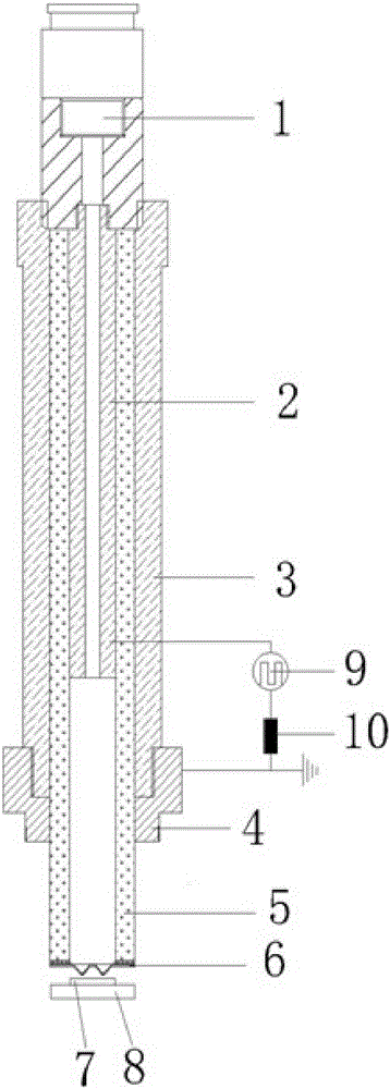
[0051] see figure 1 , the present embodiment is an atmospheric pressure plasma nozzle micro-nano jet device for parallel scanning plasma processing, which is composed of an atmospheric pressure plasma nozzle, a needle tip array with micro-nano nozzles and a three-dimensional mobile platform. The atmospheric pressure plasma nozzle is composed of an air inlet 1, an anode metal tube 2, an insulating tube 3, a cathode metal ring 4 and a quartz tube 5. The material of the insulating tube 3 can be an insulating material such as polytetrafluoroethylene, and the electrodes 2 and 4 The material can be a metal that is not easily oxidized, such as copper.

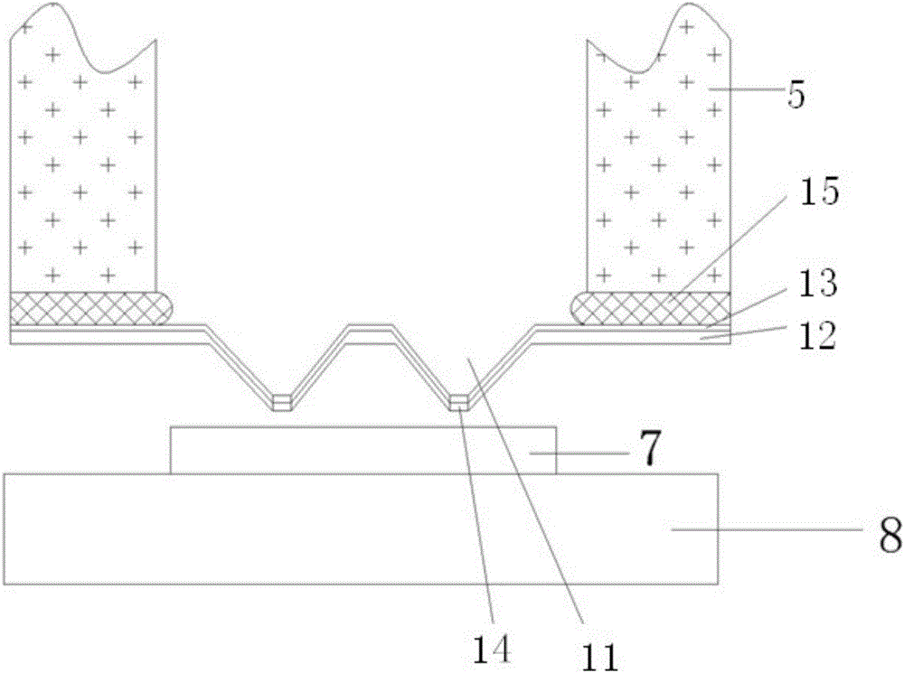
[0052] Nanonozzle tip arrays such as figure 2 As shown, it is a device with a metal layer / oxide layer two-layer structure. The substrate of the device is a single crystal silicon wafer, and an inverted pyramid-shaped cavity 11 is obtained by anisotropic etching with KOH etching solution. The surface is oxidized by wet oxygen to for...


PUM


Abstract

The invention discloses a device and method for parallel mask-less scanning micro-nano processing based on an atmospheric pressure plasma jet tube. The processing device comprises the atmospheric pressure plasma jet tube and a jet nozzle tip array integrated at the lower end of the jet tube, wherein a three-dimensional precise movable platform is disposed on the lower part of the jet nozzle tip array; the jet nozzle tip array comprises multiple jet nozzle tips which are equipped with micro-nano holes; and each jet nozzle tip is equipped with a hollow micro chamber which is shaped like an inverted pyramid. The atmospheric pressure plasma jet tube is placed in an atmospheric pressure environment; reaction gases are continuously injected into the jet tube; ionization takes place to the reaction gases under an electric field effect, so that reaction plasma is generated; and the jet nozzle tip array is used to form a plasma nano jet flow array. The three-dimensional precise movable platform controls a plasma micro jet flow device to generate motion relative to a processed sample, so that low-cost, high-precision and efficient mask-less etching, sedimentation processing and surface modification can be implemented to multiple materials. In this way, requirements for processing and application of a small batch of micro-nano devices with multiple varieties can be satisfied.

Description

technical field [0001] The invention relates to a micro-nano processing technology, in particular to a parallel maskless scanning micro-nano processing device and method based on an atmospheric pressure plasma nozzle. Background technique [0002] In the field of semiconductor technology and micro-electromechanical systems (MEMS), plasma etching and thin film deposition technology has high etching rate, good etching selectivity and good uniformity of thin film deposition. The reactive gas can process specific materials, and the solid product generated by the reactive gas discharge can be deposited on the surface of the sample to realize the advantages of thin film deposition, so it has been widely used. In practical applications, it is often necessary to etch and process patterns of different depths and shapes on the surface of the sample. In traditional plasma etching, macroscopic plasma is used, that is, the plasma acts on the entire sample surface. If selective etching i...

Claims


Application Information

Patent Timeline
IPC IPC(8): H01J37/32B82Y30/00B82Y40/00
CPCB82Y30/00B82Y40/00H01J37/32082H01J37/32807
Inventor 文莉戴一川
Owner UNIV OF SCI & TECH OF CHINA
Why Eureka
Try Eureka