A kind of graphene strip-shaped electron injection field emission cold cathode and its production method
A strip-shaped electron and graphene technology, applied in the direction of electron emission electrode/cathode, X-ray tube cold cathode, cold cathode, etc., can solve the problem of limited output power, high electric field strength of conductor sheets, and the inability to stack several conductor sheets in parallel to improve Output power and other issues, to achieve the effect of lower working voltage, easy industrial production, and less defects
- Summary
- Abstract
- Description
- Claims
- Application Information
AI Technical Summary
Problems solved by technology
Method used
Image
Examples
Embodiment 1
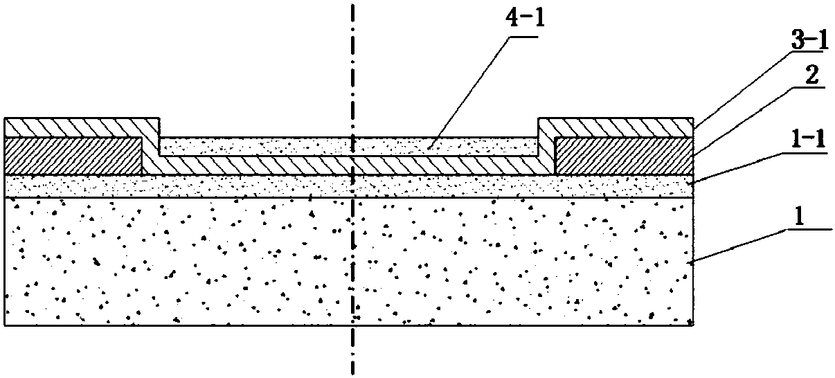
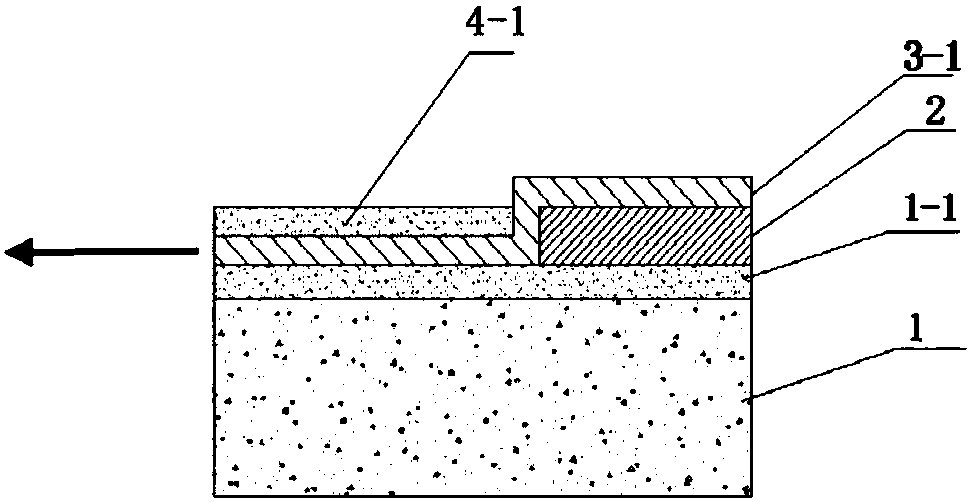
[0029] In this example, two silicon oxides covered with Si surface are produced at one time. 2 SiO 2 / Si is used as the substrate, and a layer of graphene film is used as the emitter of the band-shaped electron injection field emission cold cathode as an example. The production method is as follows:
[0030] Step 1. SiO 2 After the / Si substrate is cleaned and dried, it is ready for use;
[0031] Step 2. The preparation of graphene thin film: at first place the copper foil of 25 μm thickness in the tube furnace that diameter is 5cm, length is 100cm, in H 2 Heating to 1030°C under a protective atmosphere and keeping the temperature constant for 1.5 hours, then injecting H 2 Quantity 1 / 50 of CH 4 , CH at 900°C 4 cleavage, CH 4 After pyrolysis, the copper foil is adsorbed on the surface of the metal foil to form a graphene film with a thickness of less than 1nm. After cooling in the furnace, it is cut into graphene / copper foil blocks with a length × width of 2.2 × 2cm for u...
Embodiment 2
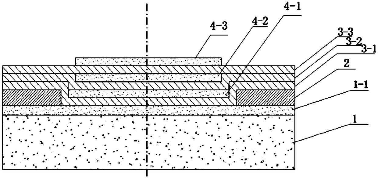
[0037] In this embodiment, the band-shaped electron injection field emission cold cathode adopting three layers of graphene as the emitter is taken as an example, and the method is as follows:
[0038] Steps one, two, three and four are all the same as in Example 1;
[0039] Step 5.a. Use the magnetron sputtering coating process to coat a layer of SiO with a thickness of 30nm and an area of about 1.79×2cm on the upper surface of the graphene facing the substrate in the single-layer emitter basic part obtained in step 4. 2 Layer is used as the insulating medium strengthening layer to obtain the cold cathode base part containing the substrate / electrode / graphene / insulating medium strengthening layer;
[0040] Step 6. The making of the multilayer emitter graphene ribbon-shaped electron injection field emission cold cathode: sequentially on the basis of the cold cathode base part containing the substrate / electrode / graphene / insulating medium reinforcement layer obtained in step 5....
Embodiment 3
[0042] In this embodiment, the strip-shaped electron injection field emission cold cathode adopting a flexible insulating material as a substrate and a three-layer graphene emitter is taken as an example:
[0043] Step 1. Use a polyimide film as the substrate 1, and clean and dry the substrate before use;
[0044] All the other steps 2, 3, 4, 5 and 6 are the same as in Example 2; Figure 5 , Image 6 That is, the structural schematic diagram of the cold cathode basic part obtained in the fifth step of this embodiment and the structural schematic diagram of the strip-shaped electron injection field emission cold cathode using a flexible insulating material as the substrate and having a three-layer graphene emitter.
PUM
| Property | Measurement | Unit |
|---|---|---|
| thickness | aaaaa | aaaaa |
| thickness | aaaaa | aaaaa |
| thickness | aaaaa | aaaaa |
Abstract
Description
Claims
Application Information


