Photoelectric thin film capable of strengthening adhesive force and application of photoelectric thin film

A technology that enhances adhesion and photoelectric thin films, applied in circuits, electrical components, semiconductor devices, etc., can solve the problems of great harm to the human body and the environment, achieve the effect of improving adhesion and overcoming easy fall-off

Inactive Publication Date: 2016-11-09
EAST CHINA NORMAL UNIV
View PDF2 Cites 20 Cited by
  • Summary
  • Abstract
  • Description
  • Claims
  • Application Information

AI Technical Summary

Problems solved by technology

HF is a strong corrosive acid, which is extremely harmful to the human body and the environment, and needs to be handled carefully.

Method used


Image

  • Photoelectric thin film capable of strengthening adhesive force and application of photoelectric thin film
  • Photoelectric thin film capable of strengthening adhesive force and application of photoelectric thin film
  • Photoelectric thin film capable of strengthening adhesive force and application of photoelectric thin film

Examples


preparation example Construction

[0023] In a specific embodiment, the preparation method of the present invention includes the following specific steps: select a high-transparency glass substrate, first clean the glass surface with a cleaning process, then roughen the glass surface with NaOH solution, and then dry it. Then, the interface modification layer is deposited by coating technology, dried or annealed, and then the metal layer is vacuum-coated.

[0024] Preferably, the metal or metal alloy thin film layer can be prepared by magnetron sputtering, vacuum thermal evaporation, electron beam evaporation and laser deposition, and can also be prepared by printing, printing and spin coating. For preparing the photoelectric thin film layer, first cover one, two or more interface modification layers on the substrate, and then vacuum deposit the metal thin film layer. In order to improve the adhesion between the substrate and the interface modification layer, the interface modification layer and the metal film l...

Embodiment 1

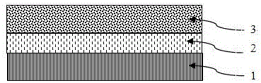
[0030] Such as figure 1 As shown, the photoelectric thin film with enhanced adhesion in this embodiment includes a substrate 1 , an interface modification layer 2 and a metal thin film layer 3 in sequence from bottom to top. Wherein, the substrate 1 is glass, the interface modification layer 2 is aluminum oxide, and the metal thin film layer 3 is silver film. A single specific material is given in this embodiment, which does not limit the choice of other materials, but is just an example to illustrate the present invention. The glass surface of the substrate 1 is subjected to surface roughening and / or surface plasma treatment, an alumina precursor is prepared by a sol-gel method, and then an alumina interface modification layer 2 is coated on the substrate, followed by thermal evaporation or magnetron sputtering Deposit silver film 3. The structure of the product prepared in this embodiment is Glass / AlOx / Ag. The photoelectric thin film prepared in this embodiment can be use...

Embodiment 2

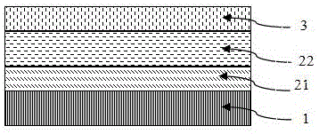
[0032] Such as figure 2As shown, the transparent conductive film of this embodiment includes a substrate 1 , a first interface modification layer 21 , a second interface modification layer 22 and a metal thin film layer 3 from bottom to top. Wherein, the substrate 1 is glass, the first interface modification layer 21 is a silicon oxide layer, the second interface modification layer 22 is a titanium oxide layer, and the metal thin film layer 3 is a silver film layer or a silver-titanium alloy. This embodiment gives a single specific material, does not limit the choice of other materials, and is just to illustrate the present invention. Manufacturing process is with embodiment 1. The glass surface of the substrate 1 is subjected to surface roughening and / or surface plasma treatment, and silicon oxide and titanium oxide precursors are prepared by using a sol-gel method, and then silicon oxide is respectively coated on the substrate as the first layer 21 of interface modificatio...


PUM

PropertyMeasurementUnit
thicknessaaaaaaaaaa
thicknessaaaaaaaaaa
reflectanceaaaaaaaaaa

Abstract

The invention discloses a photoelectric thin film capable of strengthening the adhesive force. A thin film structure comprises a substrate, one, two or multiple interface modification layers and a metal thin film layer, wherein the interface modification layers are the same or different in material; the substrate is a glass, quartz, lead-containing glass, ceramic, zirconium oxide, aluminum oxide, silicon wafer, mica or plastic substrate; the interface modification layers are made of silicon oxide, aluminum oxide, zirconium oxide, titanium oxide or a compound of two or more of the silicon oxide, the aluminum oxide, the zirconium oxide and the titanium oxide; and the metal thin film layer is made of aluminum, silver, copper, gold and various metal alloys. Each interface modification layer is prepared by CVD, PVD or a chemical method such as a sol-gel method; and the metal thin film layer is prepared by the methods of PVD, CVD or chemical plating and the like. After the interface modification layers are adopted, the adhesion properties of the substrate and the metal thin film layer are obviously improved; the disadvantage that the metal thin film layer easily falls off on the substrate is well overcome; and the photoelectric thin film can be applied to the fields of a photoelectric device electrode, a light reflector or an anti-electromagnetic interference protective layer and the like.

Description

technical field [0001] The invention belongs to the field of photoelectric thin films, and in particular relates to a photoelectric thin film with enhanced adhesion and its application in photoelectric devices. Background technique [0002] Metal electrodes represented by aluminum, copper, silver, and gold usually have common optoelectronic properties such as high conductivity and high reflectivity, and are widely used in solar cells, flat-panel displays, electronic circuits, optical mirrors, and other optoelectronic devices and optoelectronics Thin films and anti-electromagnetic waves and other fields. Metallic silver has been widely used in coating fields such as solar cells, display fields, reflectors and crystal glass due to its high reflectivity and moderate price. However, the chemical activity of gold, silver or copper is low, and it is difficult to form a good chemical bond with the substrate. It is usually necessary to increase the interface roughness to enhance th...

Claims


Application Information

Patent Timeline
Patent Type & Authority Applications(China)
IPC IPC(8): H01L31/0224
CPCH01L31/022425
Inventor 陈晓红
Owner EAST CHINA NORMAL UNIV
Why Eureka
Try Eureka