

Preparation method of crystalline silicon solar cell textured structure
A technology of solar cells and crystalline silicon, applied in the field of solar cells, can solve the problems of crystal flower comparison, short life, poor uniformity, etc., and achieve the improvement of open circuit voltage and short circuit current, stability and uniformity, and photoelectric conversion efficiency Improved effect
- Summary
- Abstract
- Description
- Claims
- Application Information
AI Technical Summary
Problems solved by technology
Method used
Image

Examples
Embodiment 1
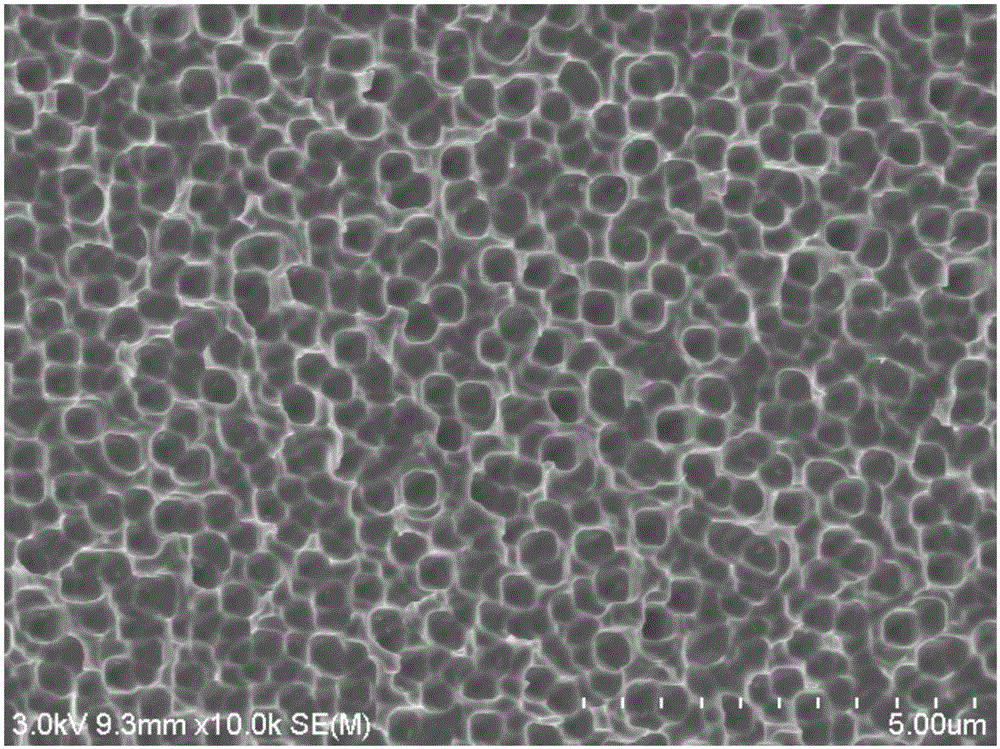
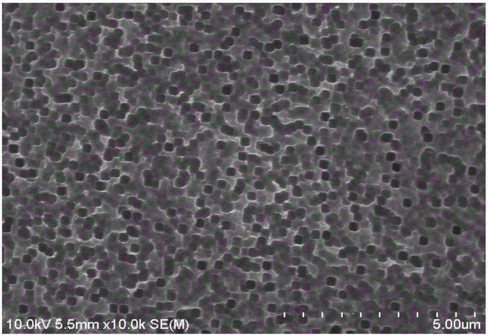
[0041] see figure 1 Shown, a kind of preparation method of textured structure of crystalline silicon solar cell comprises the steps:
[0042] (1) Put the silicon wafer into a hydrofluoric acid solution containing an oxidizing agent and a metal salt to form a porous layer structure; the temperature is 50°C, and the time is 10-1000s;
[0043] (2) washing with water;
[0044] Then use the first chemical etching solution to etch the surface; the first chemical etching solution is a mixed solution of hydrofluoric acid, nitric acid and citric acid; the temperature is 40° C., and the time is 10 minutes;
[0045] Wherein the concentration of hydrofluoric acid is 1mol / L, the concentration of nitric acid is 5mol / L, and the concentration of citric acid is 0.05mol / L;
[0046] (3) washing with water;
[0047] Then put the above-mentioned silicon chip into the second chemical etching solution for immersion to form a suede structure; the second chemical etching solution is alkaline solution...
PUM
 Abstract
Description
Claims
Application Information