Growth method of LED epitaxial contact layer

A growth method and contact layer technology, applied in the direction of electrical components, circuits, semiconductor devices, etc., can solve problems such as increased working voltage

Active Publication Date: 2016-11-09
XIANGNENG HUALEI OPTOELECTRONICS
View PDF3 Cites 8 Cited by
  • Summary
  • Abstract
  • Description
  • Claims
  • Application Information

AI Technical Summary

Problems solved by technology

[0003] However, in the traditional sapphire LED epitaxial growth, since it is difficult to form an ohmic contact between P-GaN and ITO, it is easy to increase the working voltage due to the increase of contact resistance.

Method used


Image

  • Growth method of LED epitaxial contact layer
  • Growth method of LED epitaxial contact layer
  • Growth method of LED epitaxial contact layer

Examples


Embodiment 1

[0055] The invention uses VEECO MOCVD to grow high-brightness GaN-based LED epitaxial wafers. Using high-purity H 2 or high purity N 2 or high purity H 2 and high purity N 2 The mixed gas as the carrier gas, high-purity NH 3 As N source, metal-organic source trimethylgallium (TMGa), metal-organic source triethylgallium (TEGa), trimethylindium (TMIn) as indium source, N-type dopant is silane (SiH 4 ), trimethylaluminum (TMAl) as the aluminum source, and the P-type dopant as magnesium dicene (CP 2 Mg), the substrate is (0001) sapphire, and the reaction pressure is between 100Torr and 1000Torr. The specific growth method is as follows (for the epitaxial structure, please refer to figure 1 ):

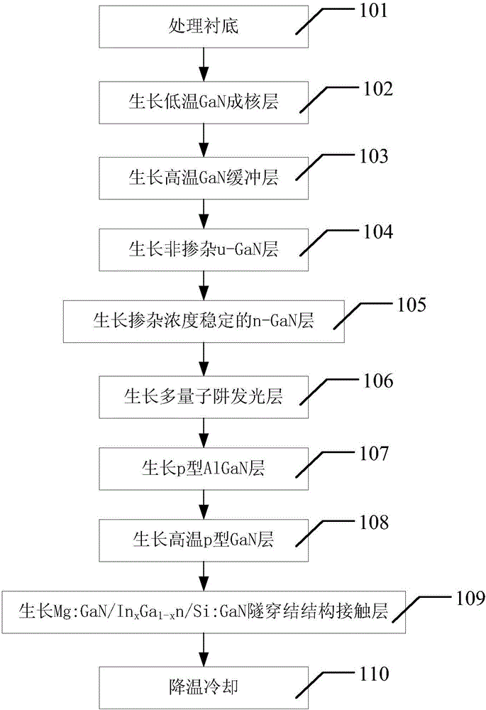
[0056] The present invention provides a LED epitaxial contact layer growth method, see figure 2 , including in turn: step 101, processing the substrate; step 102, growing a low-temperature GaN nucleation layer; step 103, growing a high-temperature GaN buffer layer; step 104, growin...

Embodiment 2

[0064] The invention uses VEECO MOCVD to grow high-brightness GaN-based LED epitaxial wafers. Using high-purity H 2 or high purity N 2 or high purity H 2 and high purity N 2 The mixed gas as the carrier gas, high-purity NH 3 As N source, metal-organic source trimethylgallium (TMGa), metal-organic source triethylgallium (TEGa), trimethylindium (TMIn) as indium source, N-type dopant is silane (SiH 4 ), trimethylaluminum (TMAl) as the aluminum source, and the P-type dopant as magnesium dicene (CP 2 Mg), the substrate is (0001) sapphire, and the reaction pressure is between 100Torr and 1000Torr. The specific growth method is as follows (for the epitaxial structure, please refer to figure 1 ):

[0065] 1. Treat the substrate, specifically:

[0066] H at 1050°C-1150°C 2 atmosphere, the sapphire is annealed and the substrate surface is cleaned.

[0067] 2. Growth of low-temperature GaN nucleation layer, specifically:

[0068] Cool down to 500°C-620°C, feed NH 3 and TMGa, ...


PUM


Abstract

The application discloses a growth method of an LED epitaxial contact layer. The method comprises: processing a substrate; a growing a low-temperature GaN nucleating layer; growing a high-temperature GaN buffer layer; growing a non-doping u-GaN layer; growing a n-GaN layer with stable doping concentration; growing a multi-quantum-well light-emitting layer; growing a p type AlGaN layer; growing a high-temperature p type GaN layer; growing a Mg:GaN/InxGa(1-x)n/Si:GaN tunneling structure contact layer; and carrying out temperature-reducing cooling. According to the technical scheme, the contact layer of LED epitaxy is designed to have a Mg:GaN/InxGa(1-x)n/Si:GaN tunneling structure, so that the contact resistance is reduced effectively and thus the working voltage of the LED chip is reduced.

Description

technical field [0001] The present application relates to the technical field of LED epitaxial design application, in particular, to a method for growing an LED epitaxial contact layer. Background technique [0002] At present, LED (Light Emitting Diode, light-emitting diode) is a kind of solid-state lighting. Its advantages such as small size, low power consumption, long service life, high brightness, environmental protection, and durability are recognized by consumers, and the scale of domestic production of LEDs is gradually expanding. ; The demand for LED brightness and luminous efficacy is increasing day by day in the market. How to grow better epitaxial wafers has been paid more and more attention. Because of the improvement of the quality of epitaxial layer crystals, the performance of LED devices can be improved, and the luminous efficiency, life, anti-aging ability, The antistatic ability and stability will increase with the improvement of the crystal quality of the...

Claims


Application Information

Patent Timeline
Patent Type & Authority Applications(China)
IPC IPC(8): H01L33/00
CPCH01L33/007
Inventor 林传强
Owner XIANGNENG HUALEI OPTOELECTRONICS
Why Eureka
Try Eureka