LED purple light epitaxial structure of vertical structure and preparation method thereof

A technology of vertical structure and epitaxial structure, applied in electrical components, circuits, semiconductor devices, etc., can solve the problems of low luminous efficiency, high manufacturing cost, and low yield of purple LED chips, and achieve wide adjustment range, uniform distribution ratio, Effect of improving internal quantum efficiency

Active Publication Date: 2016-11-16
CHINA UNITED NORTHWEST INST FOR ENG DESIGN & RES
View PDF5 Cites 3 Cited by
  • Summary
  • Abstract
  • Description
  • Claims
  • Application Information

AI Technical Summary

Problems solved by technology

[0003] At present, the epitaxial growth technology of purple light LED is not mature enough. On the one hand, it is restricted by the characteristics of the purple light growth material, and on the other hand, due to the influence of the energy band structure of the purple light LED, the luminous efficiency of the current purple light LED chip is low, the preparation cost is high, and the difficulty is great. , low yield, etc.

Method used


Image

  • LED purple light epitaxial structure of vertical structure and preparation method thereof

Examples


Embodiment 1

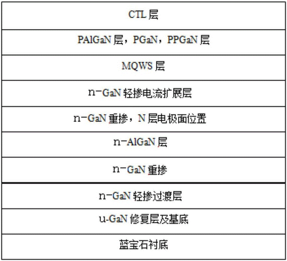
[0056] A preparation method for vertical structure LED ultraviolet light epitaxy, comprising the following steps:

[0057] Step 1: Pass N at a temperature of 1070°C and a pressure of 150torr 2 Baking for 10 minutes, nitrided sapphire, SiC or Si substrate, the substrate thickness is 430μm;

[0058] Step 2: Cool down the sapphire, SiC or Si substrate after nitriding in step 1 to 515°C and a pressure of 800torr, then grow a substrate with a thickness of 15nm on the substrate, then raise the temperature to 1030°C and a pressure of 400torr to regenerate the substrate Crystallization, and then grow a 1.8μm u-GaN repair layer;

[0059] Step 3: Raise the temperature to 1070°C and the pressure is 200torr to grow a lightly Si-doped n-GaN layer with a thickness of 500nm, and then grow a heavily Si-doped n-GaN layer with a thickness of 300nm;

[0060] Step 4: growing an n-AlGaN current spreading layer on the basis of the heavily Si-doped n-GaN layer, with a thickness of 80 nm;

[0061]...

Embodiment 2

[0069] A preparation method for vertical structure LED ultraviolet light epitaxy, comprising the following steps:

[0070] Step 1: Pass N at a temperature of 1080°C and a pressure of 150torr 2 Baking for 20 minutes, nitrided sapphire, SiC or Si substrate, the substrate thickness is 440μm;

[0071] Step 2: Cool down the sapphire, SiC or Si substrate after nitriding in step 1 to 525°C and a pressure of 800torr, then grow a substrate with a thickness of 25nm on the substrate, then raise the temperature to 1040°C and a pressure of 400torr to regenerate the substrate Crystallization, and then grow a 2.1μm u-GaN repair layer;

[0072] Step 3: Raise the temperature to 1080°C and the pressure is 200torr to grow a lightly Si-doped n-GaN layer with a thickness of 550nm, and then grow a heavily Si-doped n-GaN layer with a thickness of 350nm;

[0073] Step 4: growing an n-AlGaN current spreading layer on the basis of the heavily Si-doped n-GaN layer, with a thickness of 160 nm;

[0074...

Embodiment 3

[0082] A preparation method for vertical structure LED ultraviolet light epitaxy, comprising the following steps:

[0083] Step 1: Pass N at a temperature of 1090°C and a pressure of 150torr 2 Baking for 30min, nitrided sapphire, SiC or Si substrate, the substrate thickness is 450μm;

[0084] Step 2: Cool down the sapphire, SiC or Si substrate after nitriding in step 1 to 535°C, and the pressure is 800torr, and then grow a substrate with a thickness of 35nm on the substrate, and then raise the temperature to 1050°C, and the pressure is 400torr to regenerate the substrate. Crystallization, and then grow a 2.5μm u-GaN repair layer;

[0085] Step 3: Raise the temperature to 1090°C and the pressure is 200torr to grow a lightly Si-doped n-GaN layer with a thickness of 600nm, and then grow a heavily Si-doped n-GaN layer with a thickness of 400nm;

[0086] Step 4: growing an n-AlGaN current spreading layer on the basis of the heavily Si-doped n-GaN layer, with a thickness of 240 nm...


PUM

PropertyMeasurementUnit
Thicknessaaaaaaaaaa
Thicknessaaaaaaaaaa
Thicknessaaaaaaaaaa

Abstract

The invention discloses an LED purple light epitaxial structure of a vertical structure and a preparation method thereof. The preparation method comprises the following steps: using ammonia gas, high-purity trimethyl indium (TMIn), TMAl, TEGa and high-purity trimethyl gallium (TMGa) as sources respectively, using SiH4 and Cp2Mg as an n-type doping agent and a p-type doping agent respectively, using hydrogen or nitrogen as carrier gas, introducing the carrier gas into a reaction chamber to perform a chemical reaction with the ammonia gas at the temperature of 900-1100 DEG C, generating a three-five compound semiconductor, and depositing on sapphire, a silicon wafer, a silicon carbide sheet or a quartz glass sheet according to a certain lattice sequence to prepare the epitaxial structure. The components, doping concentration, thickness and the like of the epitaxial layer can be controlled by accurately controlling the flow and on-off time of a gas source, the regulating range of growth rate is relatively wide, and the relatively high growth rate can be applicable to batch growth.

Description

【Technical field】 [0001] The invention belongs to the technical field of semiconductors, and in particular relates to a vertical structure LED ultraviolet epitaxial structure and a preparation method thereof. 【Background technique】 [0002] With the advancement of science and technology and the development of new energy sources, solid-state LED lighting will become the trend of lighting in the future world. Due to the advantages of energy saving, environmental protection, safety, long life, low consumption, and low heat, LEDs have been widely used in traffic lights, traffic lights, etc. Signal lights, landscape decorative lights, display screens, car tail lights, mobile phone backlights and other fields. At present, the LEDs on the market are mainly blue-green light, followed by red and yellow light. There are relatively few purple and ultraviolet LED products, mainly because purple LEDs are difficult to manufacture and have low luminous efficiency. With the development of ...

Claims


Application Information

Patent Timeline
IPC IPC(8): H01L33/00H01L33/12H01L33/32
CPCH01L33/007H01L33/12H01L33/32
Inventor 田进刘波波田伟赵俊李谊
Owner CHINA UNITED NORTHWEST INST FOR ENG DESIGN & RES
Why Eureka
Try Eureka