Semiconductor double-stage surface structure laser machining method based on electronic dynamic regulating and control

A technology of electronic dynamic control and dual-level surface structure, which is applied in the field of femtosecond laser applications, can solve the problems of short processing cycle, low repeatability, and high cost, and achieve the effects of short processing cycle, good repeatability, and convenient operation

Active Publication Date: 2016-12-14
BEIJING INSTITUTE OF TECHNOLOGYGY
View PDF12 Cites 17 Cited by
  • Summary
  • Abstract
  • Description
  • Claims
  • Application Information

AI Technical Summary

Problems solved by technology

[0004] The purpose of the present invention is to solve the problems of long processing cycle, high cost, low efficiency and small repeatability existing in the processing of multi-level structures in the existing processing methods, and to expand the application field of femtosecond laser pro

Method used


Image

  • Semiconductor double-stage surface structure laser machining method based on electronic dynamic regulating and control
  • Semiconductor double-stage surface structure laser machining method based on electronic dynamic regulating and control

Examples


Embodiment Construction

[0026] The present invention will be further described below in conjunction with the accompanying drawings and embodiments.

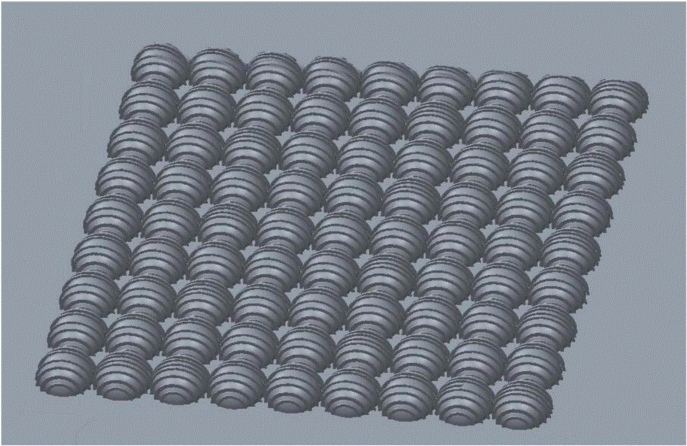
[0027] A method for electronically dynamic regulation and control of laser processing of semiconductor double-level surface structures, the specific steps are as follows:

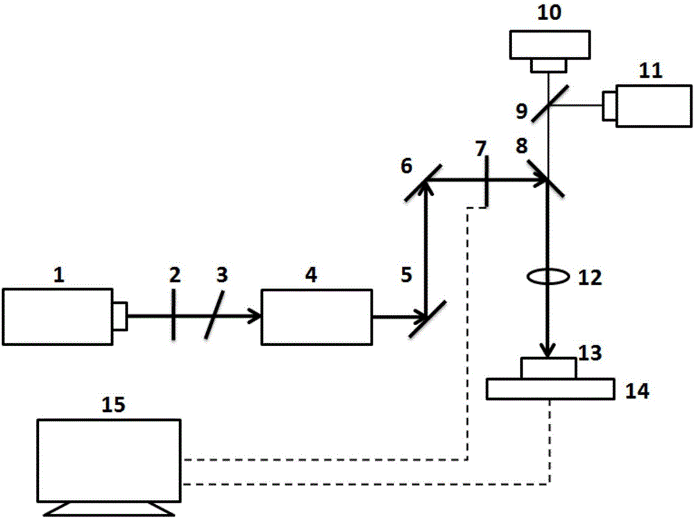
[0028] Step 1. The femtosecond laser produces a femtosecond pulse laser with a center wavelength of 800nm, and uses a pulse time domain shaping device to shape the femtosecond pulse laser into a femtosecond laser double pulse sequence, and the sub-pulse energy ratio is 1:1;

[0029] Step 2. The femtosecond laser double pulse sequence obtained in step 1 is vertically incident on the surface of the sample, and focused by a plano-convex lens (f=100mm), and the focal point of the focused laser reaches the surface of the sample;

[0030] Step 3. Drop water into the Petri dish where the sample is placed, so that it is about 3mm below the sample;

[0031] Step 4. Find the focus again in th...


PUM


Abstract

The invention relates to a semiconductor double-stage surface structure laser machining method based on electronic dynamic regulating and control, and belongs to the technical field of femtosecond laser application. Under the water-assisted condition, a time domain shaping pulse sequence is designed, the local-area instantaneous electronic density and electronic temperature are adjusted, the phase change process of a material is changed, and therefore a micro-nano composite double-stage structure is obtained. Compared with a traditional multistage structure machining method, the method for machining the semiconductor multi-stage structure through the time domain shaping pulse sequence has the beneficial effects of being short in period, low in cost and good in repeatability.

Description

technical field [0001] The invention relates to a method for processing a double-level surface structure of a semiconductor based on electronic dynamic regulation and control of a laser, and belongs to the technical field of femtosecond laser applications. Background technique [0002] Since scholars discovered that the double-level structure of lotus leaf is the key factor for its superhydrophobic and self-cleaning properties, people have been working on the processing of multi-level structures and trying to obtain functional surfaces. There are various methods for processing multilevel structures, including chemical vapor deposition, electrochemical methods, reactive ion beam etching, photolithography, and laser processing. Among them, laser processing is widely used because of its advantages of wide application range, high efficiency, high repetition rate and low cost. [0003] At present, laser processing of multi-level structures is mainly limited to obtaining multi-le...

Claims


Application Information

Patent Timeline
IPC IPC(8): B23K26/064B23K26/70B81C1/00
CPCB23K26/0622B23K26/0643B23K26/702B81C1/00015
Inventor 姜澜孟革李欣许永达
Owner BEIJING INSTITUTE OF TECHNOLOGYGY
Why Eureka
Try Eureka