Copper indium gallium selenide thin-film solar cell uniform in gallium distribution and preparation method thereof
A solar cell and element uniform technology, which is applied to circuits, photovoltaic power generation, electrical components, etc., can solve the problems of poor gallium on the surface of copper indium gallium selenide films, uneven distribution of gallium elements, and two-phase separation of films, and achieves favorable diffusion. Penetration, uniform distribution, increased surface area effect
- Summary
- Abstract
- Description
- Claims
- Application Information
AI Technical Summary
Problems solved by technology
Method used
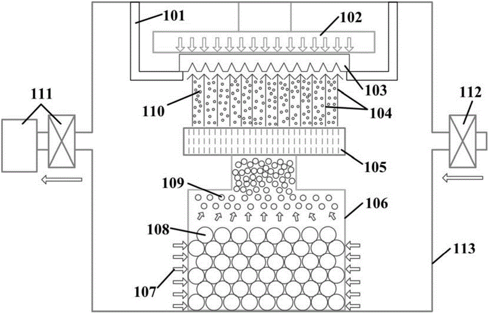
Image

Examples
Embodiment 1
[0031] (1) Clean the surface of soda-lime glass with a semiconductor cleaning agent, then soak it in deionized water and ultrasonically clean it for 30 minutes, twice before and after, take it out, rinse it with deionized water, and finally dry it with nitrogen;
[0032] (2) Place the cleaned soda-lime glass in 2×10 -4 In the Pa vacuum chamber, the molybdenum back electrode is sputtered by sputtering method, with a thickness of 730nm;
[0033] (3) On the soda-lime glass sputtered with molybdenum back electrode, the copper layer is electrodeposited by the pulsed direct current method, the pulse frequency is 3000Hz, the duty cycle is 5%, and the current density is 55mA / cm 2 , the time is 13s, the solution system used contains CuSO 4 and H 2 SO 4 The mixed solution (CuSO in the mixed solution 4 The concentration is 0.75mol / L, H 2 SO 4 The concentration is 0.765mol / L);
[0034] (4) On the copper layer obtained in step (3), use pulsed direct current method to electrodeposit ...
Embodiment 2
[0042] (1) Clean the surface of soda-lime glass with a semiconductor cleaning agent, then soak it in deionized water and ultrasonically clean it for 30 minutes, twice before and after, take it out, rinse it with deionized water, and finally dry it with nitrogen;
[0043] (2) Place the cleaned soda-lime glass in 2×10 -4 In the Pa vacuum chamber, the molybdenum back electrode is sputtered by sputtering method, with a thickness of 730nm;
[0044] (3) On the soda-lime glass sputtered with molybdenum back electrode, the copper layer is electrodeposited by the pulsed direct current method, the pulse frequency is 3000Hz, the duty cycle is 5%, and the current density is 55mA / cm 2 , the time is 13s, the solution system used contains CuSO 4 and H 2 SO 4 The mixed solution (CuSO in the mixed solution 4 The concentration is 0.75mol / L, H 2 SO 4 The concentration is 0.765mol / L);
[0045] (4) On the copper layer obtained in step (3), use pulsed direct current method to electrodeposit ...
Embodiment 3
[0053] (1) Clean the surface of soda-lime glass with a semiconductor cleaning agent, then soak it in deionized water and ultrasonically clean it for 30 minutes, twice before and after, take it out, rinse it with deionized water, and finally dry it with nitrogen;
[0054] (2) Place the cleaned soda-lime glass in 2×10 -4 In the Pa vacuum chamber, the molybdenum back electrode is sputtered by sputtering method, with a thickness of 730nm;
[0055] (3) On the soda-lime glass sputtered with molybdenum back electrode, the copper layer was electrodeposited by the pulsed direct current method, the pulse frequency was 4000Hz, the duty cycle was 10%, and the current density was 57.5mA / cm 2 , the time is 12s, the solution system used contains CuSO 4 and H 2 SO 4 The mixed solution (CuSO in the mixed solution 4 The concentration is 0.75mol / L, H 2 SO 4 The concentration is 0.765mol / L);
[0056] (4) On the copper layer obtained in step (3), use the pulsed direct current method to elec...
PUM
| Property | Measurement | Unit |
|---|---|---|
| thickness | aaaaa | aaaaa |
| conversion efficiency | aaaaa | aaaaa |
| conversion efficiency | aaaaa | aaaaa |
Abstract
Description
Claims
Application Information