Thin film transistor and preparation method thereof
A thin-film transistor and thin-film layer technology, which is applied in the direction of transistors, semiconductor/solid-state device manufacturing, electrical components, etc., can solve the problems of increasing the cost of thin-film transistors, achieve the effects of reducing technology costs, simplifying the preparation process, and broad application prospects
- Summary
- Abstract
- Description
- Claims
- Application Information
AI Technical Summary
Problems solved by technology
Method used
Image

Examples
Embodiment 1
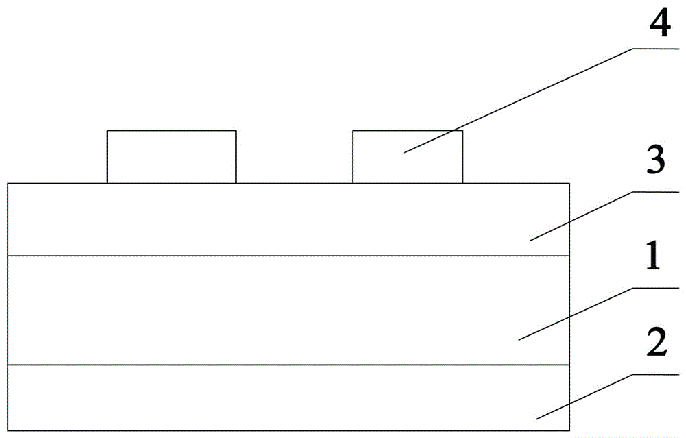
[0028] This embodiment provides a method for preparing a thin film transistor, using PET plastic with a thickness of 50 microns as the insulating substrate layer. The method specifically includes the following steps:
[0029] (1) Clean the PET insulating substrate layer and place it in the magnetron sputtering growth chamber. Under the condition of low-pressure high-purity argon gas with a gas pressure of 5 Pa, use radio frequency magnetron sputtering to deposit the PET insulating substrate layer An ITO conductive thin film layer with a thickness of 60 nm was prepared on the bottom side as the gate electrode, and the sputtering power was controlled at 100 W.
[0030] (2) In a low-pressure pure oxygen environment with a gas pressure of 10 Pa, a pulsed laser with a pulsed laser energy of 100 mJ and a pulsed laser frequency of 5 Hz is used to bombard the high-purity InGaZnO ceramic target, and the resulting plasma plume is deposited on the On the other side of the PET insulating ...
Embodiment 2
[0036] This embodiment provides a method for preparing a thin film transistor, using glass with a thickness of 50 microns as the insulating substrate layer, and the specific preparation steps are roughly the same as those in Embodiment 1, except that:
[0037] The step of preparing the metal oxide semiconductor thin film layer and the source-drain electrodes on the surface of the other side of the insulating substrate layer includes:
[0038] First, fix the metal mask with source and drain electrode patterns on the surface of the glass insulating substrate layer, and fix it in the thermal evaporation coating chamber, under a vacuum pressure of less than 1×10 -4 Under the condition of Pa, an aluminum film with a thickness of 35 nm was prepared on the surface of the other side of the glass insulating substrate layer by thermal evaporation coating method as the transistor source and drain electrode layer, wherein the evaporation current controlled by thermal evaporation coating t...
Embodiment 3
[0042] This embodiment provides a method for preparing a thin film transistor, using paper with a thickness of 75 microns as the insulating substrate. The specific preparation steps are roughly the same as those in Example 1, except that:
[0043] When preparing the metal oxide semiconductor thin film on the other side surface of the insulating substrate layer, in this embodiment, a ZnO thin film is used as the metal oxide semiconductor thin film layer.
[0044] The structure of a thin film transistor prepared by the above preparation method provided in this embodiment is the same as that in Embodiment 1.
PUM
| Property | Measurement | Unit |
|---|---|---|
| Thickness | aaaaa | aaaaa |
| Thickness | aaaaa | aaaaa |
| Thickness | aaaaa | aaaaa |
Abstract
Description
Claims
Application Information
PatSnap Eureka turns technology decisions into work you can execute. Powered by our Innovation Knowledge Graph, it runs expert workflows across engineering, life sciences, materials and intellectual property. Get your review-ready output in minutes.


