

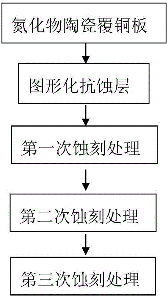
Patterning method of nitride ceramic copper-clad plate and nitride ceramic copper-clad plate
A technology of nitride ceramics and copper clad laminates, which is applied in the manufacture of electrical components, electrical solid devices, semiconductor/solid devices, etc., can solve the problems of poor state of the metal plate surface, reduced etching ability, slow etching rate, etc., and achieve the state of the plate surface Good, uniform etching, shortened etching time
- Summary
- Abstract
- Description
- Claims
- Application Information
AI Technical Summary
Problems solved by technology
Method used
Image

Examples
preparation example Construction
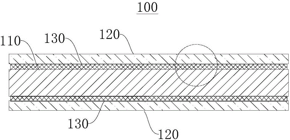
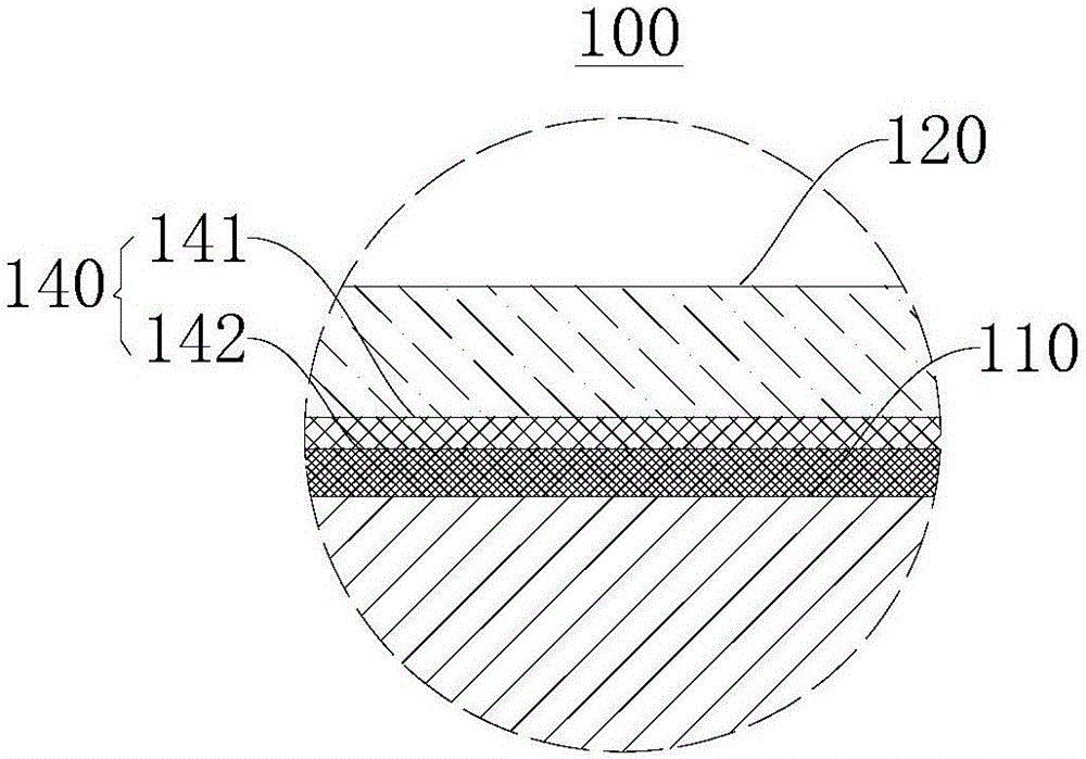
[0034]The preparation of the nitride ceramic copper-clad laminate 100 further includes: a printing process, a copper-clad foil process, and a sintering process. Specifically: the printing process is to apply the active brazing material to both surfaces of the ceramic substrate 110 by full-plate printing. In this embodiment, the active brazing material of the present invention is copper-silver brazing material, and further includes one or more active metals such as titanium, zirconium, and hafnium. The copper foil cladding process is to coat a whole plate of copper foil 120 on both sides of the ceramic substrate 110 coated with active solder, wherein the copper foil 120 requires surface pretreatment, that is, degreasing and deoxidation treatment to ensure that the surface of the copper foil 120 is free from grease and oxides. According to a preferred embodiment, the degreasing of the copper foil 120 can be carried out by lye or degreasing agent. According to a preferred embod...
Embodiment 1
[0050] The active brazing material is coated on both sides of the 50mm×50mm aluminum nitride ceramic substrate 110 by full plate printing. A piece of copper foil 120 matching the size of the ceramic substrate 110 is provided on both sides of the ceramic substrate 110 coated with active solder. Before the copper foil 120 is installed, the surface of the copper foil 120 needs to be pre-treated to remove oil stains and oxide layers on the surface. The aluminum nitride ceramic substrate 110 and the copper foil 120 are sintered at a temperature of 800° C., and the sintering process is carried out under vacuum conditions with a vacuum degree of 5×10 -4 Pa. The whole sintering time is 10min. After sintering, the surface of the semi-finished aluminum nitride ceramic copper-clad laminate 100 is provided with a dry film as a resist layer. Then a desired etching pattern (that is, a circuit pattern to be formed) is formed on the resist layer. The semi-finished aluminum nitride ceramic...
Embodiment 2
[0053] The active brazing material is coated on both sides of the 50mm×50mm boron nitride ceramic substrate 110 by full plate printing. A piece of copper foil 120 matching the size of the ceramic substrate 110 is provided on both sides of the ceramic substrate 110 coated with active solder. Before the copper foil 120 is installed, the surface of the copper foil 120 needs to be pre-treated to remove oil stains and oxide layers on the surface. The aluminum nitride ceramic substrate 110 and the copper foil 120 are sintered at a temperature of 900° C., and the sintering process is carried out under vacuum conditions with a vacuum degree of 2×10 -4 Pa. The whole sintering time is 40min. After sintering, the surface of the semi-finished aluminum nitride ceramic copper-clad laminate 100 is provided with a dry film as a resist layer. Then a desired etching pattern (that is, a circuit pattern to be formed) is formed on the resist layer. The semi-finished aluminum nitride ceramic co...
PUM
 Abstract
Description
Claims
Application Information