Solar battery sheet and assembly thereof
A technology of solar cells and conductive layers, which is applied in the field of solar cells, can solve the problems of adverse effects on the lifespan of silicon chips, serious absorption of high-energy photons, and small emitter bandgap, and achieve simple structure, increased built-in electric field, and battery performance. Enhanced effect
- Summary
- Abstract
- Description
- Claims
- Application Information
AI Technical Summary
Problems solved by technology
Method used
Image
Examples
Embodiment Construction
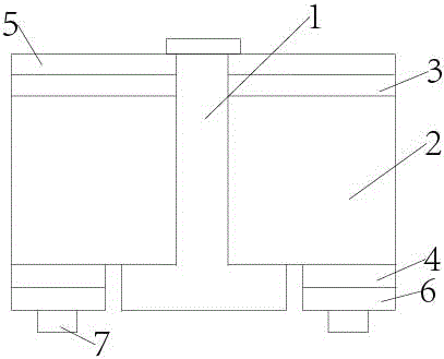
[0023] Such as figure 1 Shown is the original basic structure of the MWT cell, including the front electrode 1 and the substrate 2; the upper surface of the substrate 2 is provided with an emitter 3, and the lower surface of the substrate 2 is provided with a back field doped layer 4; the emitter 3 is provided with An antireflection layer 5 ; a back passivation layer 6 is arranged under the back field doped layer 4 ; a back electrode 7 is arranged under the back passivation layer 6 .
[0024] The present invention will be further described in detail below in conjunction with the accompanying drawings and specific embodiments.
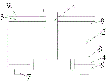
[0025] The present invention uses hydrogen-containing amorphous silicon oxide as the tunneling layer 8 to passivate the upper and lower surfaces of the substrate 2, then uses amorphous silicon carbide as the emitter 3, and uses hydrogen-containing microcrystalline silicon as the back field doped layer 4, and then PVD (Physical Vapor Deposition) method ...
PUM
 Abstract
Description
Claims
Application Information
 - R&D
- Intellectual Property
- Life Sciences
- Materials
- Tech Scout
- Unparalleled Data Quality
- Higher Quality Content
- 60% Fewer Hallucinations
Browse by: Latest US Patents, China's latest patents, Technical Efficacy Thesaurus, Application Domain, Technology Topic, Popular Technical Reports.
© 2025 PatSnap. All rights reserved.Legal|Privacy policy|Modern Slavery Act Transparency Statement|Sitemap|About US| Contact US: help@patsnap.com


