Micronano array structure, fabrication method thereof and preparation of mask array for micronano array structure

An array structure, micro-nano technology, applied in the field of preparing the mask array and its preparation, can solve the problems of time-consuming and labor-intensive processing cost, inability to meet the fast processing, inability to meet the requirements, and achieve convenient processing and large-area fast processing. Finished, smooth surface

Active Publication Date: 2017-02-22
THE NAT CENT FOR NANOSCI & TECH NCNST OF CHINA
View PDF3 Cites 5 Cited by
  • Summary
  • Abstract
  • Description
  • Claims
  • Application Information

AI Technical Summary

Problems solved by technology

However, these technologies and methods are not only time-consuming and labor-intensive, but also greatly increase the processing cost, which cannot meet the needs of actual production, processing and preparation, especially the needs of large-area rapid processing.

Method used


Image

  • Micronano array structure, fabrication method thereof and preparation of mask array for micronano array structure
  • Micronano array structure, fabrication method thereof and preparation of mask array for micronano array structure
  • Micronano array structure, fabrication method thereof and preparation of mask array for micronano array structure

Examples


Embodiment 1

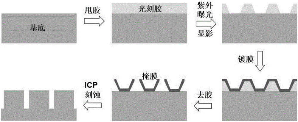
[0061] A method for preparing a micro-nano array structure, comprising the steps of:

[0062] (1) Provide a silicon carbide substrate with a thickness of 330 μm;

[0063] (2) Spin-coat a 2 μm thick UV photoresist on the silicon carbide substrate, and then bake for 5 minutes;

[0064] (3) Use a UV lithography machine to expose the UV photoresist according to a predetermined circular pattern for 40 seconds, and develop it in a developer for 40 seconds;

[0065] (4) Plating 400nm copper with electron beam evaporation coating instrument;

[0066] (5) Putting into an acetone solution to remove the ultraviolet photoresist to obtain a mask array;

[0067] (6) Using reactive ion etching for 10 minutes, transfer the columnar array structure to the silicon carbide substrate, precisely control the structural height of the micron column, and obtain the micronano array structure;

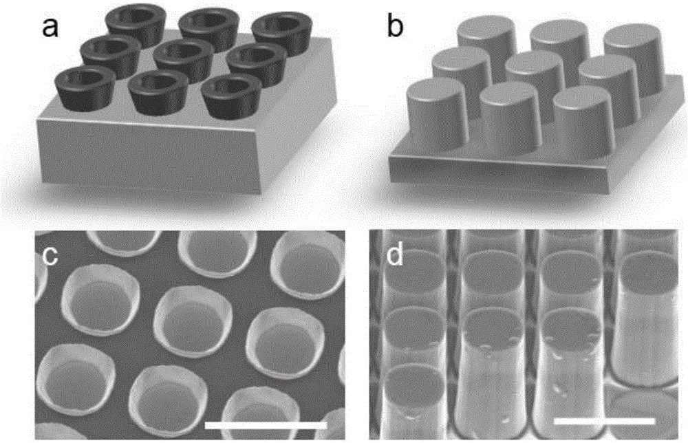
[0068] The schematic diagram of the prepared circular mask array is shown in figure 2 a, SEM image as sh...

Embodiment 2

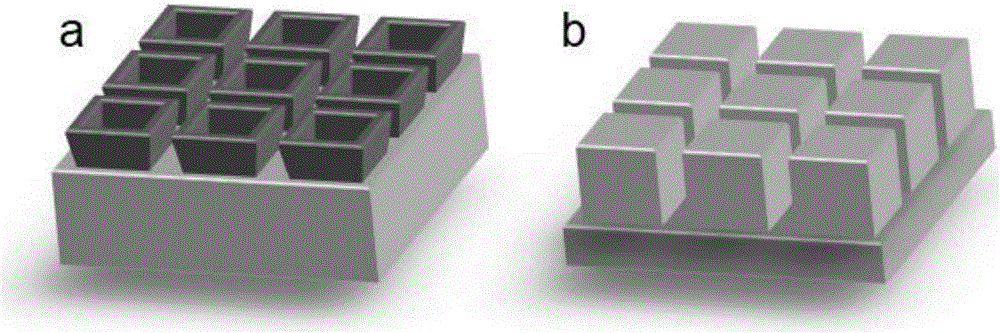
[0070] A method for preparing a micro-nano array structure, the only difference from Example 1 is that the predetermined pattern is different, which is a square shape. According to the preparation method of Example 1, the period of the prepared mask array is 8 μm, and the upper surface edge of the warped edge The length is 6 μm, the height is 2 μm; the micro-nano array structure is a steep and smooth square cylinder with a period of 8 μm, a side length of 6 μm, and a height of 14.5 μm.

[0071] The schematic diagram of the prepared square mask array is shown in image 3 a, Schematic diagram of the square column structure of the micro-nano array. image 3 b.

Embodiment 3

[0073] A method for preparing a micro-nano array structure, the only difference from Example 1 is that the predetermined pattern is different, which is a regular cross (the regular cross is a cross-shaped structure with 12 sides, and the lengths of each side are equal), according to According to the preparation method of Example 1, the period of the prepared mask array is 8 μm, the side length of the upper surface of the raised edge is 6 μm, and the height is 2 μm; the micro-nano array structure is a straight and smooth cylinder, the period is 8 μm, and the side length is 2 μm. 6 μm and a height of 14.5 μm.

[0074] The schematic diagram of the prepared cross-shaped mask array is shown in Figure 4 a, Schematic diagram of the cross-shaped column structure of the micro-nano array. Figure 4 b.


PUM

PropertyMeasurementUnit
thicknessaaaaaaaaaa
thicknessaaaaaaaaaa
thicknessaaaaaaaaaa

Abstract

The invention provides a mask array for fabricating a micronano array structure on a substrate and the micronano array structure obtained by fabrication of the mask array. The mask array comprises arrayed mask units, wherein the mask unit comprises a bottom surface and a side surface upwards tiling, and the bottom surface is laid on the substrate. With the mask array provided by the invention, the defects such as distortion, side wall stripes and cylinder steepness reduction due to a boundary effect during transferring a mask shape to the substrate caused by that mask damage such as deformation, defect and shrinkage of a traditional mask in dry etching is easy to generate are overcome, and a suspension mask provided by the invention is free from limitation of materials and shapes; meanwhile, the steep smooth-surface cylinder is also free from the limitation of materials and shapes; and the mask array is simple in process flow, is convenient to process and is relatively low in cost.

Description

technical field [0001] The invention belongs to the technical field of micro-nano processing, and in particular relates to a micro-nano array structure and a mask array for preparing it, in particular to a highly steep micro-nano array structure and a preparation method thereof, and a method for preparing the same Mask array and method of making the same. Background technique [0002] Traditional dry etching techniques generally require masks, and the preparation of masks usually uses photolithography and coating methods. The traditional mask is generally a planar mask that is closely attached to the substrate. During the dry etching process, the edge of the mask will be bombarded by ion etching gas and cause damage including defects, distortion and shrinkage, resulting in mask morphology Sidewall effects such as distortion, sidewall striations, and drop in steepness can occur during transfer to the substrate. [0003] In response to the above problems, some methods have b...

Claims


Application Information

Patent Timeline
Patent Type & Authority Applications(China)
IPC IPC(8): G03F1/20B81B7/02B81C1/00
CPCB81B7/02B81C1/00388G03F1/20
Inventor 陈东学刘前
Owner THE NAT CENT FOR NANOSCI & TECH NCNST OF CHINA
Why Eureka
Try Eureka