Chemical method for semiconductor film materials of ternary wide bandgap compound of synthesis of copper-zinc iodide

A thin film material and chemical method technology, applied in the field of material chemistry, can solve the problems of large environmental impact, high reaction temperature, complicated operation, etc., and achieve the effects of simple reaction device, simple operation and controllable reaction process.

Active Publication Date: 2017-02-22
XUCHANG UNIV
View PDF2 Cites 11 Cited by
  • Summary
  • Abstract
  • Description
  • Claims
  • Application Information

AI Technical Summary

Problems solved by technology

At present, the preparation methods of multi-component compound semiconductors are constantly developing, but the methods commonly used

Method used


Image

  • Chemical method for semiconductor film materials of ternary wide bandgap compound of synthesis of copper-zinc iodide
  • Chemical method for semiconductor film materials of ternary wide bandgap compound of synthesis of copper-zinc iodide
  • Chemical method for semiconductor film materials of ternary wide bandgap compound of synthesis of copper-zinc iodide

Examples


Embodiment 1

[0041] 1. Preparation work: ultrasonically clean ordinary glass with detergent and deionized water for 20 minutes in turn, and then use concentrated ammonia water (25% by mass) / hydrogen peroxide (30% by mass) / deionized water (volume ratio 1:2) :5) of the mixed solution at 80°C for 30min, and finally ultrasonically cleaned with deionized water for 20min. The treated ordinary glass was dried at 80°C and stored in a clean desiccator for later use. A copper-zinc alloy layer with a thickness of 100 nm was sputtered on an ordinary glass substrate by magnetron sputtering technology, and the film thickness was controlled by film thickness monitoring (FTM). The obtained ordinary glass with a copper-zinc alloy layer was stored in a desiccator for use.

[0042] 2. Reaction steps: The ordinary glass sputtered with a copper-zinc alloy layer with a thickness of 100nm was placed in an airtight container filled with iodine vapor and reacted at 45°C for 8 hours. The resulting product is a ...

Embodiment 2

[0044] 1. Preparation: Same as Example 1, sputtering a copper-zinc alloy layer with a thickness of 100 nm on a common glass substrate.

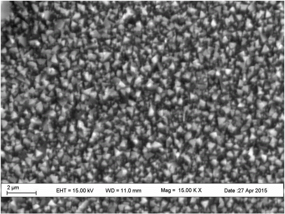
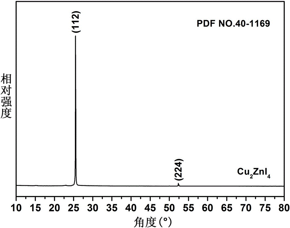
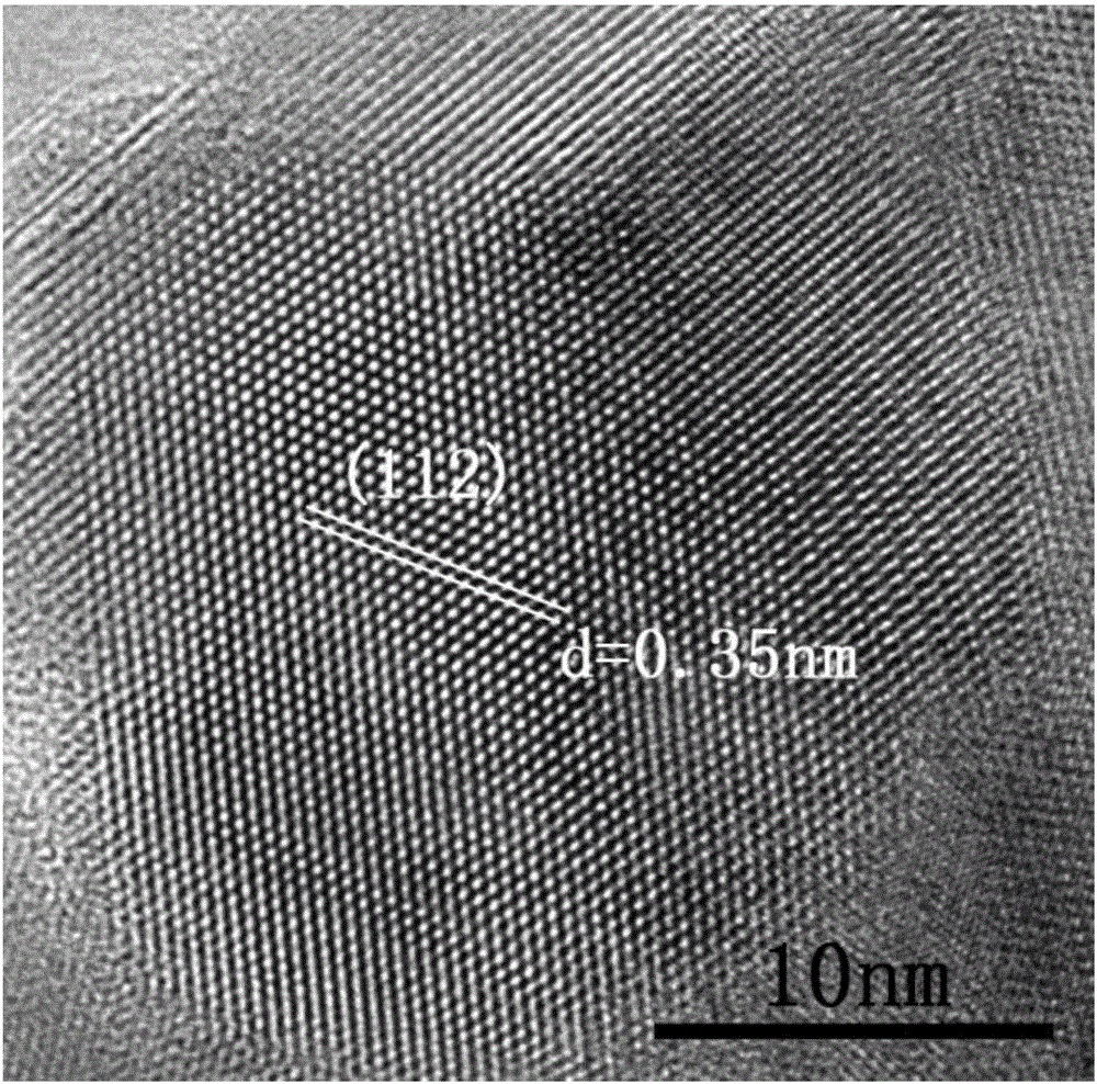
[0045] 2. Reaction steps: The ordinary glass sputtered with a 100nm copper-zinc alloy layer was placed in an airtight container filled with iodine vapor and reacted at 60°C for 5 hours. The resulting product is a white film. Figure 4 is the SEM photo of the obtained sample, the surface of the film is mainly composed of flaky particles; Figure 5 is the XRD pattern of the obtained sample, and the diffraction peak shown in the figure is Cu 2 ZnI 4 The (112) and (224) crystal planes of (112) and (224) crystal planes show that it has a strong (112) crystal plane dominant orientation.

Embodiment 3

[0047] 1. Preparation: Same as Example 1, sputtering a copper-zinc alloy layer with a thickness of 100 nm on a common glass substrate.

[0048]2. Reaction steps: The ordinary glass sputtered with a 100nm copper-zinc alloy layer was placed in a closed container filled with iodine vapor and reacted at 70°C for 3 hours. The resulting product is a white film. Image 6 It is the SEM photo film of the obtained sample, and the surface is mainly composed of flakes and irregular particles; Figure 7 is the XRD pattern of the obtained sample, and the diffraction peak shown in the figure is Cu 2 ZnI 4 The (112) and (224) crystal planes of (112) and (224) crystal planes show that it has a strong (112) crystal plane dominant orientation.


PUM


Abstract

The invention belongs to chemical technical field, in particular to a chemical method for semiconductor film materials of ternary wide bandgap compound of synthesis of copper-zinc iodide. The method is that putting the copper-zinc alloy film into iodine vapor with a temperature of 45 DEG C to 80 DEG C for co-oxidation reaction of the copper-zinc alloy. The reaction time takes 3 to 8 hours. After reacting for certain time, Cu2ZnI4 films can be produced in situ on the surface of substrate, and that is the semiconductor film materials of the synthesis of the copper-zinc iodide. The preparation method does not require organic solvents to participate in the reaction or reaction medium. The crystal is crystallized well. The product can be used directly without complicated processing. The method has the advantages of simple operation, rapid reaction, better environmental protection, low energy consumption, low cost and good reproducibility. In addition, a film can be directly formed on the substrate surface in the method. The material is more beneficial for the application in photoelectric conversion devices.

Description

[0001] Technical field: [0002] The invention belongs to the technical field of material chemistry, in particular to a chemical method for synthesizing a copper-zinc iodide ternary wide-bandgap compound semiconductor thin film material. [0003] Background technique: [0004] Wide-bandgap semiconductors are generally semiconductor materials with a bandgap greater than 2.0 eV at room temperature, so they can transmit most of the sunlight and are widely used in the neighborhood of optoelectronic devices. In recent years, new solar cells with low-cost and high-efficiency lead halide perovskite materials as light absorbing layers have developed rapidly, and their photoelectric conversion efficiency has exceeded 20%, which is expected to be applied in solar energy utilization. But lead halide-based perovskite solar cell devices need to use expensive wide-bandgap organic compounds (Sprio-MEOTAD, P3HT, etc.) as hole transport layer materials. The price of these organic compounds is a...

Claims


Application Information

Patent Timeline
IPC IPC(8): H01L21/02
CPCH01L21/02425H01L21/02521H01L21/02614
Inventor 雷岩谷龙艳贾祖孝路凯张磊磊铁伟伟郑直
Owner XUCHANG UNIV
Why Eureka
Try Eureka