

Synthesis method and application of nano-silver/silica Raman surface enhanced thin film
A silicon dioxide and surface-enhanced technology, applied in Raman scattering, filament/wire forming, single-component synthetic polymer rayon, etc., can solve the problem of poor repeatability of results, unfavorable popularization and application, and complicated preparation process, etc. Problems, to achieve good experimental repeatability, wide application, easy to remove the effect
- Summary
- Abstract
- Description
- Claims
- Application Information
AI Technical Summary
Problems solved by technology
Method used
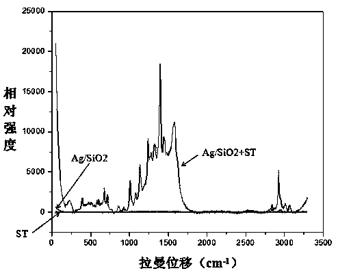
Image


Examples
Embodiment 1
[0018] The synthesis method of nano silver / silicon dioxide Raman surface enhanced film is:
[0019] Step 1: Preparation of spinning solution: Weigh 2g of PVP with a molecular weight of 1.3 million and dissolve it in 30mL of ethanol, stir magnetically for 2 hours, slowly add 2.23mL tetraethyl orthosilicate dropwise, stir for 4 hours to obtain solution A, and then Dissolve 0.085g of silver nitrate in 5mL of water, then slowly add it dropwise to solution A, and stir for 24 hours;
[0020] The second step: at a temperature of 20°C and a humidity of 55%, the positive voltage of the electrospinning is controlled to be 16KV, the negative voltage is -3KV, the spinning distance is 20cm, and the spinning speed is 0.4mm / min. Liquid spinning is made into thin film material, irradiated by fluorescent lamp, and left to stand for 6 hours;
[0021] Step 3: Remove the film, put it in a vacuum drying oven, dry at 30°C for 24 hours, then calcinate at 550°C for 3 hours, and cool naturally.
[0...
Embodiment 2
[0024] The synthesis method of nano silver / silicon dioxide Raman surface enhanced film is:
[0025] Step 1: Preparation of spinning solution: Weigh 2g of PVP with a molecular weight of 2 million and dissolve it in 50mL of ethanol, stir magnetically for 2 hours, slowly add 6mL tetraethyl orthosilicate dropwise, stir for 4 hours to obtain solution A, then take Dissolve 0.6g of silver nitrate in 6mL of water, then slowly add it dropwise to solution A, and stir for 24 hours;
[0026] The second step: at a temperature of 22°C and a humidity of 60%, control the positive voltage of electrospinning to 16KV, the negative voltage to -3KV, the spinning distance to 20cm, and the spinning speed to 0.6mm / min. Liquid spinning is made into thin film material, irradiated by fluorescent lamp, and left to stand for 6 hours;
[0027] Step 3: Remove the film, put it in a vacuum drying oven, dry it at 30°C for 24 hours, then calcinate it at 500°C for 3 hours, and cool it naturally.
[0028] The d...
Embodiment 3
[0030] The synthesis method of nano silver / silicon dioxide Raman surface enhanced film is:
[0031] Step 1: Preparation of spinning solution: Weigh 2g of PVP with a molecular weight of 500,000 and dissolve it in 20mL of ethanol, stir magnetically for 2 hours, slowly add 2mL tetraethyl orthosilicate dropwise, stir for 4 hours to obtain solution A, then take Dissolve 0.3g of silver nitrate in 5mL of water, then slowly add it dropwise to solution A, and stir for 24 hours;
[0032] The second step: at a temperature of 18°C and a humidity of 50%, control the positive voltage of electrospinning to 8KV, the negative voltage to -3KV, the spinning distance to 20cm, and the spinning speed to 0.6mm / min. Liquid spinning is made into thin film material, irradiated by fluorescent lamp, and left to stand for 6 hours;
[0033] Step 3: Remove the film, put it in a vacuum drying oven, dry it at 30°C for 24 hours, then calcinate it at 700°C for 3 hours, and cool it naturally.
[0034] The di...
PUM
| Property | Measurement | Unit |
|---|---|---|
| particle diameter | aaaaa | aaaaa |
| size | aaaaa | aaaaa |
| size | aaaaa | aaaaa |
Abstract
Description
Claims
Application Information