Organic electrode resistive random access memory and preparation method thereof

A resistive variable memory and organic electrode technology, applied in the direction of electrical components, etc., can solve the problems of poor durability and data memory characteristics, poor storage performance, unstable resistance change, etc., and achieve simple and easy preparation methods and high storage performance. The effect of stability and concentrated resistance distribution

Active Publication Date: 2017-04-26
HEBEI UNIVERSITY
View PDF4 Cites 4 Cited by
  • Summary
  • Abstract
  • Description
  • Claims
  • Application Information

AI Technical Summary

Problems solved by technology

[0005] The object of the present invention is to provide an organic electrode resistive variable memory and its preparation method to solve the problems of unstable resistance change, poor storage performance, poor durability and data memory characteristics of existing organic resistive variable memory devices

Method used


Image

  • Organic electrode resistive random access memory and preparation method thereof
  • Organic electrode resistive random access memory and preparation method thereof
  • Organic electrode resistive random access memory and preparation method thereof

Examples


Embodiment 1

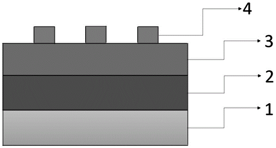
[0033] The structure of the resistive memory prepared by the present invention is as follows: figure 1 As shown, including the bottom substrate 1, the PCBM organic electrode dielectric layer 2 bonded on the substrate 1, and the Zr grown on the PCBM organic electrode dielectric layer 2 0.5 f 0.5 o 2 Resistive switching layer 3, Zr 0.5 f 0.5 o 2 An Ag electrode layer 4 grown on the resistive switching layer 3 .

[0034] Wherein the substrate 1 can be an FTO substrate or a glass substrate, and the thickness of the PCBM organic electrode dielectric layer 2 is 10~300nm; Zr 0.5 f 0.5 o 2 The thickness of the resistive switching layer 3 is 3-50 nm.

[0035] Wherein the thickness of Ag electrode layer 4 can be in the range of 50nm~200nm; Ag electrode layer 4 includes several evenly distributed in Zr 0.5 f 0.5 o 2 A circular electrode with a diameter of 80-300 μm on the resistive switching layer 3 .

Embodiment 2

[0037] The preparation method of the resistive memory provided by the present invention comprises the following steps:

[0038] (1) Wipe the surface of the FTO substrate with absorbent cotton dipped in acetone and absolute ethanol in sequence to wipe off small particles such as dust attached to the surface, and initially remove the oil on the surface, and then place the FTO substrate on the acetone Use ultrasonic cleaning for 10 minutes, then put it into alcohol and use ultrasonic cleaning for 10 minutes, then take it out with a clip, put it in deionized water and use ultrasonic cleaning for 5 minutes, then take it out, and use N 2 blow dry;

[0039] (2) Dissolve 10mg of PCBM in 1mL of chloroform, mix well, and then filter the obtained solution with a 0.22 micron filter to obtain PCBM solution; start to load the sample, open the cover of the plastic machine, turn on the vacuum pump, and wash the 1. The dried FTO substrate is vacuumed and adsorbed in the middle of the tray of ...

Embodiment 3

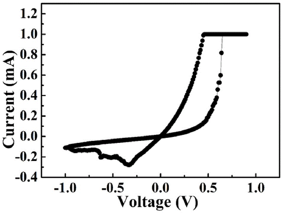
[0044] Embodiment 3 performance test

[0045] Measure its current-voltage characteristic curve by being added to the scan voltage of the resistive memory that embodiment 2 prepares, and the results are shown in image 3 . Depend on image 3 It can be seen that when the forward scanning voltage gradually increases from 0V to 1.0V, the device is in a high resistance state (lower current) at the beginning, and its resistance state gradually changes from high resistance to low when it is around 0.5V. As the voltage increases, the low resistance state reaches a stable value; after reaching the maximum scanning voltage, the scanning voltage begins to decrease gradually, when the scanning voltage continues to decrease to 0V, and then begins to scan negatively to - At about 0.35V, the off voltage is reached, and the low-resistance state is slowly and gradually transformed into a high-resistance state, and the device remains in a high-resistance state until the voltage sweeps back to...


PUM


Abstract

The invention discloses an organic electrode resistive random access memory. A PCBM organic electrode dielectric layer, a Zr<0.5>Hf<0.5>O<2> resistive conversion layer and an Ag electrode layer are formed on a substrate in turn. A preparation method of the resistive random access memory is also disclosed, comprising the following steps: cleaning and drying a substrate; spin-coating the substrate with PCBM solution and vacuum-drying the PCBM solution to form a PCBM organic electrode dielectric layer; growing a Zr<0.5>Hf<0.5>O<2> resistive conversion layer on the PCBM organic electrode dielectric layer through magnetron sputtering; and growing an Ag electrode layer on the Zr<0.5>Hf<0.5>O<2> resistive conversion layer. As a PCBM film is used as the organic electrode dielectric layer of the resistive random access memory, the resistive random access memory is different from a traditional memory prepared from oxide in that the resistive random access memory has a unique structure and good performance. Thus, the resistive random access memory has more stable storage performance, strong durability, and a wider application prospect.

Description

technical field [0001] The invention relates to a storage device and a preparation method thereof, in particular to an organic electrode resistance variable memory and a preparation method thereof. Background technique [0002] In recent years, the size of integrated circuit technology has penetrated below 20 nanometers, and traditional non-volatile memory devices have approached the physical limit. The development of a new generation of non-volatile memory has become a hot research field for scientists from all over the world. At present, the main types of non-volatile memory are magnetic memory, phase change memory and resistive change memory. Among them, resistive memory has the advantages of low power consumption, fast read and write speed, good data retention ability, simple production, and easy integration. It is a new generation of memory with great application prospects. [0003] The general structure of the resistive variable memory is a typical sandwich structure,...

Claims


Application Information

Patent Timeline
Patent Type & Authority Applications(China)
IPC IPC(8): H01L45/00
CPCH10N70/801H10N70/20H10N70/011
Inventor 闫小兵张磊赵建辉
Owner HEBEI UNIVERSITY
Why Eureka
Try Eureka