
HEMT structure with modulated carbon-doped gallium nitride high-resistance layer and preparation method of structure

A high-resistance layer, gallium nitride technology, used in semiconductor/solid-state device manufacturing, electrical components, circuits, etc., can solve the problems of deteriorating crystal quality, poor reliability and life, and high leakage current

Pending Publication Date: 2017-05-10
SOUTH CHINA UNIV OF TECH
View PDF6 Cites 14 Cited by
  • Summary
  • Abstract
  • Description
  • Claims
  • Application Information

AI Technical Summary

Problems solved by technology

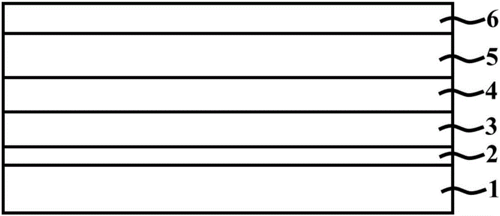
[0005] Aiming at the problems of high leakage current, poor reliability and lifespan of the existing gallium nitride-based HEMT, the present invention proposes a method to increase the resistance of the gallium nitride buffer layer without deteriorating its crystal quality, reduce the leakage current of the device, and improve the durability of the device. HEMT structure with modulated carbon-doped gallium nitride high-resistance layer with high voltage characteristics and reliability and preparation method thereof

Method used

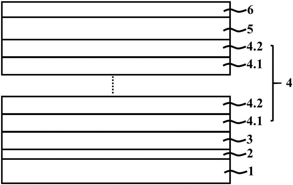
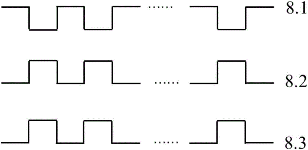

Image

  • HEMT structure with modulated carbon-doped gallium nitride high-resistance layer and preparation method of structure
  • HEMT structure with modulated carbon-doped gallium nitride high-resistance layer and preparation method of structure
  • HEMT structure with modulated carbon-doped gallium nitride high-resistance layer and preparation method of structure

Examples


Embodiment 1

[0048] A method for preparing a HEMT structure with a modulated carbon-doped gallium nitride high resistance layer, the steps are as follows:

[0049] 1) Put the sapphire substrate 1 into the metal organic chemical vapor phase chemical deposition equipment (Veco K465 type), the temperature of the substrate sheet is raised to 1100°C, the pressure is 100mbar, and hydrogen gas is introduced to clean the substrate at high temperature and remove the lining. contamination of the bottom surface;

[0050] 2) The temperature of the substrate 1 is reduced to 550° C., the pressure is increased to 550 mbar, and ammonia gas, hydrogen gas and trimethylgallium are introduced, and the flow rates are 5 liters / minute, 22 liters / minute and 30 cc respectively, as described in step 1) A 30nm GaN nucleation layer 2 is grown on the substrate to provide crystal nuclei for subsequent GaN growth.

[0051] 3) Increase the temperature of the substrate with the GaN nucleation layer 2 in step 2 to 1080° C...

Embodiment 2

[0061] A method for preparing a HEMT structure with a modulated carbon-doped gallium nitride high resistance layer, the steps are as follows:

[0062] 1) Put the sapphire substrate 1 into the metal organic chemical vapor phase chemical deposition equipment (Veco K465 type), the temperature of the substrate sheet is raised to 1050°C, the pressure is 80mbar, and hydrogen gas is introduced to clean the substrate at high temperature and remove the lining. contamination of the bottom surface;

[0063] 2) The temperature of the substrate 1 is reduced to 530° C., the pressure is increased to 530 mbar, and ammonia gas, hydrogen gas and trimethylgallium are introduced, and the flow rates are 4 liters / minute, 18 liters / minute and 25 cc respectively, as described in step 1) A 25nm GaN nucleation layer 2 is grown on the substrate to provide crystal nuclei for subsequent GaN growth.

[0064] 3) Increase the temperature of the substrate with the GaN nucleation layer 2 in step 2) to 1050° C...

Embodiment 3

[0072] A method for preparing a HEMT structure with a modulated carbon-doped gallium nitride high resistance layer, the steps are as follows:

[0073] 1) Put the sapphire substrate 1 into the metal organic chemical vapor phase chemical deposition equipment (Veco K465 type), the temperature of the substrate sheet is raised to 1150°C, the pressure is 120mbar, and hydrogen gas is introduced to clean the substrate at high temperature and remove the lining. contamination of the bottom surface;

[0074] 2) The temperature of the substrate 1 is reduced to 570° C., the pressure is increased to 570 mbar, and ammonia gas, hydrogen gas and trimethylgallium are introduced, and the flow rates are 8 liters / minute, 25 liters / minute and 35 cc respectively, as described in step 1) A 35nm GaN nucleation layer 2 is grown on the substrate to provide crystal nuclei for subsequent GaN growth.

[0075] 3) Increase the temperature of the substrate with the GaN nucleation layer 2 in step 2) to 1100° C....


PUM

PropertyMeasurementUnit
thicknessaaaaaaaaaa
thicknessaaaaaaaaaa
thicknessaaaaaaaaaa

Abstract

The invention discloses an HEMT structure with a modulated carbon-doped gallium nitride high-resistance layer and a preparation method of the structure. The HEMT structure comprises a substrate, a GaN nucleating layer, a GaN buffer layer, a GaN:C / GaN superlattice high-resistance layer and an AlGaN barrier layer from bottom to top successively, the high-resistance layer is formed by connecting GaN:C intentional doping layers and unintentional doping GaN layers alternatively, the thickness of the single GaN:C intentional doping layer is 5-500nm, and the thickness of the single unintentional doping GaN layer is 5-500nm. GaN:C / GaN superlattices can improve the resistance of a gallium nitride material but not reduce the crystal quality, and the high voltage withstanding characteristic, reliability and service life of a GaN / AlGaN heterojunction HEMT device can be improved.

Description

technical field [0001] The invention relates to a gallium nitride-based HEMT epitaxial structure, in particular to a HEMT structure with a modulated carbon-doped gallium nitride high-resistance layer and a preparation method thereof, belonging to the technical field of semiconductor microelectronics. Background technique [0002] Compared with semiconductor materials such as silicon and gallium arsenide, gallium nitride materials have stronger critical breakdown electric field, greater electron saturation drift velocity, higher band gap and thermal conductivity. The field of electronic devices has great advantages. Group-III nitride materials also have large spontaneous and piezoelectric polarization coefficients, which can be used to prepare high-electron mobility transistor devices, which can be used in the fields of high-voltage and high-power switching devices and high-frequency microwave devices. [0003] figure 1 It is a schematic diagram of the GaN-based HEMT epitax...

Claims


Application Information

Patent Timeline
Patent Type & Authority Applications(China)
IPC IPC(8): H01L29/778H01L29/06H01L21/335
CPCH01L29/0603H01L29/0684H01L29/0688H01L29/66462H01L29/7786
Inventor 徐明升王洪周泉斌
Owner SOUTH CHINA UNIV OF TECH
Learn More