

Semiconductor-laser narrow pulse driving circuit and working method thereof
A drive circuit and narrow pulse technology, which is applied in the direction of semiconductor lasers, lasers, laser components, etc., can solve the problem of inability to achieve sub-nanosecond pulse width optical pulse signal output, increase signal rise and fall time, and increase system complexity problems such as high degree of accuracy, and achieve the effect of adjustable pulse width and repetition frequency, large driving current, and simple structure
- Summary
- Abstract
- Description
- Claims
- Application Information
AI Technical Summary
Problems solved by technology
Method used
Image

Examples
Embodiment 1
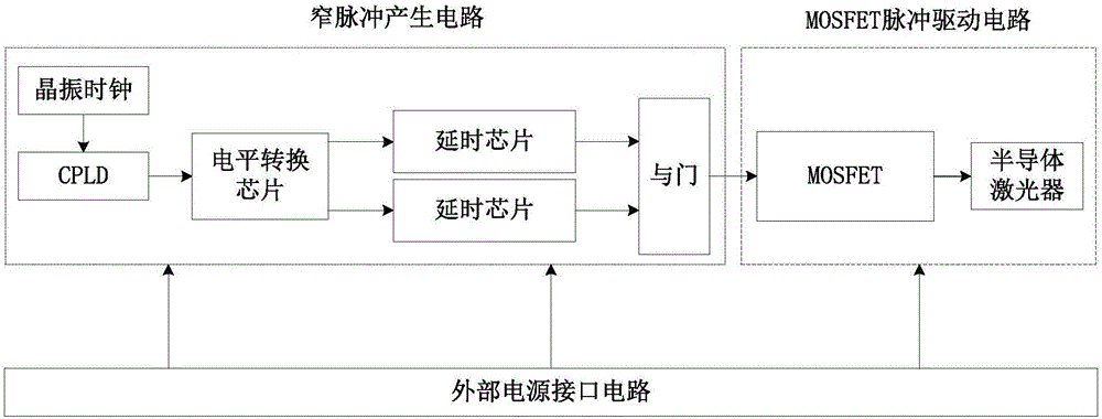
[0042] Such as figure 1 shown.
[0043] A semiconductor laser narrow pulse driving circuit, comprising an external power supply interface circuit, a narrow pulse generating circuit and a MOSFET pulse driving circuit; the external power supply interface circuit provides power for the narrow pulse generating circuit and the MOSFET pulse driving circuit respectively.
[0044] The external power supply interface circuit is used to connect with the input terminal of the external power supply and introduce the external power supply; the narrow pulse generating circuit is used to generate the required narrow pulse signal to control the MOSFET switch in the MOSFET driving circuit; the MOSFET pulse driving circuit is used to drive the laser , provide the working voltage and working current of the semiconductor laser, and drive the laser to generate the required optical pulse signal.
Embodiment 2
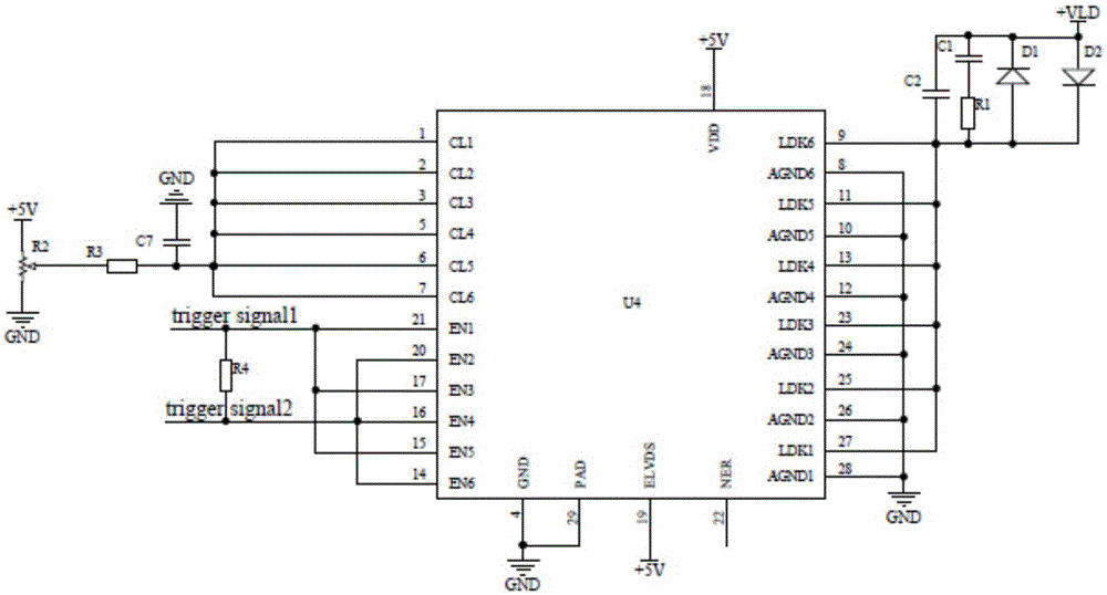
[0046] As the semiconductor laser narrow pulse drive circuit described in Embodiment 1, the difference is that the narrow pulse generation circuit includes a CPLD control chip U6, an AND gate chip U7, a crystal oscillator clock U8, a delay chip U9, a delay chip U10 and A level conversion chip U11; the MOSFET pulse drive circuit includes a MOSFET drive chip U4;
Embodiment 3
[0048] Such as Figure 6-11 shown.
[0049] As the semiconductor laser narrow pulse drive circuit described in embodiment 2, the difference is that the No. 2 pin of the crystal oscillator clock U8 is connected to the No. 12 pin of the CPLD control chip U6, and the No. 1 pin of the crystal oscillator clock U8 is connected to +3.3V Power supply, pin 1 of the crystal oscillator clock U8 is also grounded through capacitor C13, and pin 4 of the crystal oscillator clock U8 is grounded;
[0050] Pins 1 and 3 of the level conversion chip U11 are grounded, pin 2 of the level conversion chip U11 is connected to +3.3V power supply, pin 4 of the level conversion chip U11 is connected to pin 26 of the CPLD control chip U6 ; Pins 10, 13, and 18 of the level conversion chip U11 are connected in parallel and then connected to a +3.3V power supply; pins 10, 13, and 18 of the level conversion chip U11 are connected in parallel and grounded through capacitors C14, C15, C16, and C17 respectively...
PUM
| Property | Measurement | Unit |
|---|---|---|
| Pulse width | aaaaa | aaaaa |
Abstract
Description
Claims
Application Information