MEMS micro-heating chip of composite structure and manufacturing method and application of chip
A composite structure and micro-heating technology, applied in micro-structure technology, micro-structure device, manufacturing micro-structure device, etc., can solve the problems of support strength and impact resistance constraints, difficult application of membrane support, and stress-prone devices, etc. Achieve the effect of improving mechanical properties, high yield and increasing thickness
- Summary
- Abstract
- Description
- Claims
- Application Information
AI Technical Summary
Problems solved by technology
Method used
Image
Examples
Embodiment 1
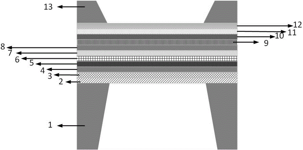
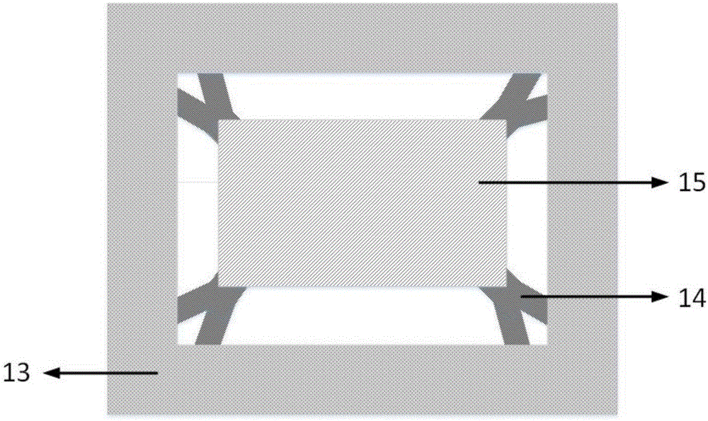
[0113] The manufacturing method of the MEMS micro-heating chip of a kind of composite structure in the present embodiment is as follows:
[0114] The first part is to prepare the lower half structure of the micro-heating chip:
[0115] First, on a single crystal silicon substrate with a thickness of 300um, 100nm of silicon oxide is grown on its surface by thermal oxidation, as the lower insulating layer 2 of the micro-heating chip;
[0116] Then, by means of spin coating and solidification, a polyimide (PI) film layer with a thickness of 1um is covered on the lower insulating layer as the thermal insulation layer 3 of the micro-heating chip;
[0117] Subsequently, a silicon oxide thin film layer with a thickness of 150 nm is grown on the heat insulating layer by plasma vapor deposition as the lower adhesion layer 4 of the micro-heating chip;
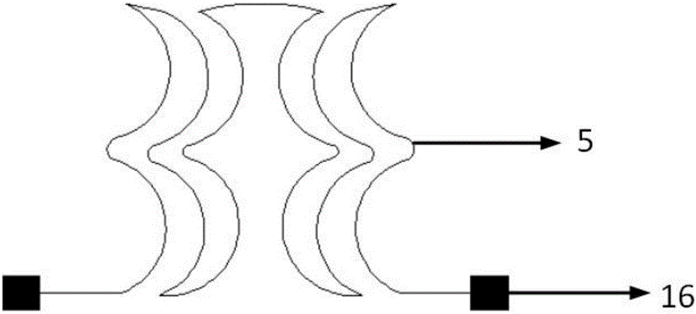
[0118] On the top of the lower adhesion layer 4, a metal Pt heating electrode layer 5 with a thickness of 200 nm is formed through pho...
Embodiment 2
[0133] The first part is to prepare the lower half structure of the micro-heating chip:
[0134] First, on a single crystal silicon substrate with a thickness of 200um, deposit 100nm of silicon oxide on its surface by means of plasma chemical vapor deposition, as the lower insulating layer 2 of the micro-heating chip;
[0135] Then, by spin coating and curing, the lower insulating layer is covered with a polyester (PET) film layer with a thickness of 1um, as the heat insulation layer 3 of the micro-heating chip;
[0136] Subsequently, a silicon oxide thin film layer with a thickness of 200nm is grown on the heat insulating layer by plasma vapor deposition as the lower adhesion layer 4 of the micro-heating chip;
[0137] On the upper surface of the lower adhesion layer, a metal W heating electrode layer 5 with a thickness of 200nm is formed through photolithography, sputtering, etching and other process steps in the semiconductor processing technology;
[0138] Then by plasma ...
Embodiment 3
[0152] The first part is to prepare the lower half structure of the micro-heating chip:
[0153] First, on a single crystal silicon substrate with a thickness of 400um, 100nm of silicon oxide is deposited on its surface by means of low-pressure chemical vapor deposition, as the lower insulating layer 2 of the micro-heating chip;
[0154] Then, by means of chemical vapor deposition, a layer of aluminum oxide with a thickness of 200nm is deposited on the lower insulating layer as the thermal insulation layer 3 of the micro-heating chip;
[0155] Subsequently, a silicon nitride thin film layer with a thickness of 200nm is grown on the heat insulating layer by plasma vapor deposition as the lower adhesion layer 4 of the micro-heating chip;
[0156] On the lower adhesion layer, a polysilicon heating electrode layer 5 with a thickness of 200nm is formed through photolithography, sputtering, etching and other process steps in the semiconductor processing technology;
[0157] Then by...
PUM
| Property | Measurement | Unit |
|---|---|---|
| thickness | aaaaa | aaaaa |
| thickness | aaaaa | aaaaa |
| thickness | aaaaa | aaaaa |
Abstract
Description
Claims
Application Information


