Preparation method and device of indium arsenide thin film material

A thin film material, a technology of indium arsenide, which is applied in the field of preparation of indium arsenide thin film materials, can solve the problems of lattice mismatch, complicated operation and complicated operation, and achieves the effect of dense film surface, obvious preferred orientation and uniform surface.

Active Publication Date: 2017-05-31
KUNMING UNIV OF SCI & TECH
View PDF0 Cites 0 Cited by
  • Summary
  • Abstract
  • Description
  • Claims
  • Application Information

AI Technical Summary

Problems solved by technology

However, because the equipment and metal-organic compounds used in MOVPE and MBE growth technologies are expensive and toxic, the production cost is high and the operation is complicated in the material preparation process, while the LPE growth technology needs to prepare a growth mother solution, which has cumbersome operations, complicated procedures, and is difficult to be effective. Removal of surface mother liquor residues and other issues
It is difficult to deposit indium arsenide thin films on single crystal Si substrates. In addition, there is a certain lattice mismatch and thermal expansion mismatch between indium arsenide and single crystal Si substrates, which will affect the deposition of indium arsenide thin films on single crystal Si substrates. Growth quality on substrate

Method used


Image

  • Preparation method and device of indium arsenide thin film material
  • Preparation method and device of indium arsenide thin film material
  • Preparation method and device of indium arsenide thin film material

Examples


Embodiment 1

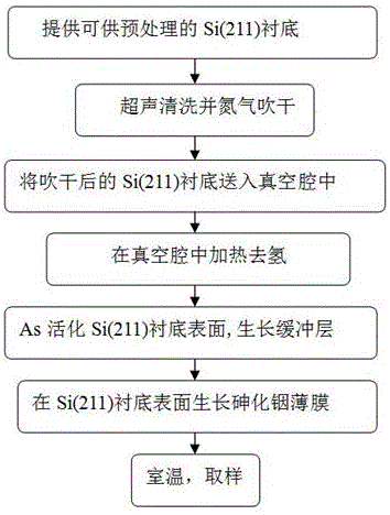
[0032] The object of the present invention is to provide a kind of preparation method of indium arsenide thin film material (such as figure 1 shown), specifically include the following steps:

[0033] (1) Cleaning of the single crystal Si(111) substrate: firstly clean the substrate with acetone for 3 min under the action of ultrasonic waves to remove oil stains and dust on the surface to prevent cracks and defects in the prepared film; then use absolute ethanol on the Wash for 3 minutes under the action of ultrasonic waves to remove residual acetone and some impurities on the surface; then use NH 4 OH, H 2 o 2 、H 2 The mixed solution of O was corroded for 3 minutes, where V NH4OH :V H2O2 :V H2O =1:2:5, then use HCl, H 2 o 2 、H 2 The mixed solution of O was corroded for 3 minutes, where V HCl :V H2O2 :VH2O =1:2:5; After taking it out, wash it alternately with a large amount of cold and hot deionized water, and then use HF, H 2 The mixed solution of O was corroded f...

Embodiment 2

[0040] The object of the present invention is to provide a method for preparing an indium arsenide thin film material, which specifically includes the following steps:

[0041] (1) Cleaning of the single crystal Si(111) substrate: first, clean with acetone for 4 minutes under the action of ultrasonic waves to remove surface oil stains and dust, so as to prevent cracks and defects in the prepared film; Wash for 4 minutes under action to remove residual acetone and some impurities on the surface; then use NH 4 OH, H 2 o 2 、H 2 The mixed solution of O was corroded for 4min, where V NH4OH :V H2O2 :V H2O =1:2:6, then use HCl, H 2 o 2 、H 2 The mixed solution of O was corroded for 4min, where V HCl :V H2O2 :V H2O =1:2:6; After taking it out, wash it alternately with a large amount of cold and hot deionized water, and then use HF, H 2 The mixed solution of O was corroded for 4min, where, V HF :V H2O =1:3; After taking it out, wash it alternately with a large amount of co...

Embodiment 3

[0048] The object of the present invention is to provide a method for preparing an indium arsenide thin film material, which specifically includes the following steps:

[0049] (1) Cleaning of the single crystal Si(111) substrate: first, wash with acetone under the action of ultrasonic waves for 5 min to remove oil stains and dust on the surface to prevent cracks and defects in the prepared film; then use absolute ethanol on the Wash for 5 minutes under the action of ultrasonic waves to remove residual acetone and some impurities on the surface; then use NH 4 OH, H 2 o 2 、H 2 The mixed solution of O was corroded for 5min, where V NH4OH :V H2O2 :V H2O =1:2:7, then use HCl, H 2 o 2 、H 2 The mixed solution of O was corroded for 5min, where V HCl :V H2O2 :V H2O =1:2:7; After taking it out, wash it alternately with a large amount of cold and hot deionized water, and then use HF, H 2 The mixed solution of O was corroded for 5 min, where, V HF :V H2O =1:5; After taking ...


PUM

PropertyMeasurementUnit
lengthaaaaaaaaaa
thicknessaaaaaaaaaa
heightaaaaaaaaaa

Abstract

The invention discloses a preparation method and device of an indium arsenide thin film material and belongs to the technical field of semiconductor manufacturing. The method comprises the steps of ultrasonically cleaning a single-side polished mono-crystalline Si substrate and drying, and then feeding the dried mono-crystalline Si substrate into a vacuum chamber for heating and dehydrogenation; heating an arsenic simple substance for volatilization, and driving As air to flow through the surface of the mono-crystalline Si substrate to form an Si-As bond; activating the surface of the mono-crystalline Si substrate, and then growing a buffer layer at a low temperature; growing an indium arsenide thin film on the surface of the mono-crystalline Si substrate; and carrying out furnace cooling to a room temperature, thereby obtaining the indium arsenide thin film material. The method is low in demands on instrument and equipment, low in cost, easy to operate and relatively good in repeatability; and the obtained indium arsenide thin film is uniform and smooth in appearance and surface, preferential growth along (111) orientation is achieved, the thickness is 4.83 microns and the crystal quality is good.

Description

technical field [0001] The invention relates to a method and a device for preparing an indium arsenide thin film material, belonging to the technical field of semiconductor manufacturing. Background technique [0002] In recent years, the research on silicon-based luminescent materials and infrared detection materials has become two hot spots in material science research. The first-generation infrared detector chip is made of narrow-band semiconductor crystal materials such as InSb and HgCdTe (MCT) represented by sphalerite structure. The detection rate of its single-tube device is extremely high, almost reaching the background detection limit. However, the integrity of their crystal structure is poor, especially a small deviation of the alloy composition will lead to a large change in the detection wavelength, especially in thin film materials, this defect is difficult to make a multi-element detector chip with a large area array. At present, the mainstream of the developm...

Claims


Application Information

Patent Timeline
Patent Type & Authority Applications(China)
IPC IPC(8): H01L21/02
CPCH01L21/02381H01L21/02485H01L21/02546H01L21/02631
Inventor 刘翔张明郭治平何利利吴长树
Owner KUNMING UNIV OF SCI & TECH
Why Eureka
Try Eureka