Low-on-resistance hydrogen terminal diamond field effect transistor and manufacturing method thereof
A field-effect transistor and low on-resistance technology, applied in the field of microelectronics, can solve the problem of large parasitic resistance in series at both ends of the channel, so as to improve saturation current and frequency characteristics, reduce on-resistance, and increase breakdown voltage Effect
- Summary
- Abstract
- Description
- Claims
- Application Information
AI Technical Summary
Problems solved by technology
Method used
Image

Examples
Embodiment
[0047] Such as Figure 1 to Figure 8 As shown, the preparation method of the low on-resistance hydrogen-terminated diamond field-effect transistor of the present invention, the steps are as follows:
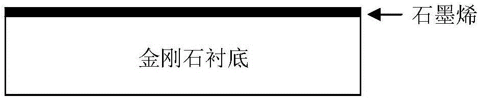
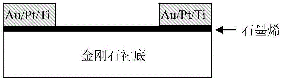
[0048] 1) Using conventional graphene transfer technology, transfer a layer of graphene film on the hydrogen-terminated single crystal diamond substrate;
[0049] 2) Perform photolithography and development of the source-drain pattern on the sample, evaporate the Au / Pt / Ti source-drain metal, and peel off with acetone solution, then pass through acetone and ethanol solutions in sequence, clean with deionized water, and blow dry with nitrogen;
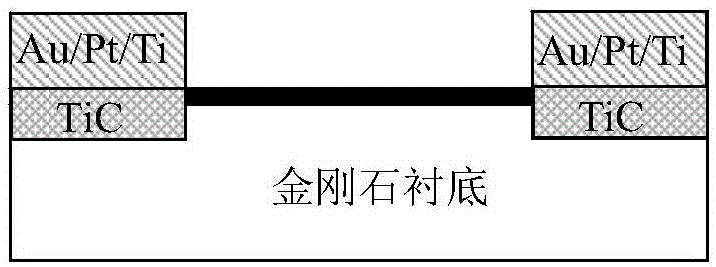
[0050] 3) The sample was annealed at 600°C for 1 hour in a hydrogen atmosphere, and the underlying metal Ti reacted with graphene and diamond to form TiC, achieving low-ohmic contact;
[0051] 4) Using atomic layer deposition (ALD) technology to grow 50nm thick Al 2 o 3 Passivating the protective layer while preventing subsequent hydroge...
PUM
| Property | Measurement | Unit |
|---|---|---|
| Thickness | aaaaa | aaaaa |
Abstract
Description
Claims
Application Information
 - Generate Ideas
- Intellectual Property
- Life Sciences
- Materials
- Tech Scout
- Unparalleled Data Quality
- Higher Quality Content
- 60% Fewer Hallucinations
Browse by: Latest US Patents, China's latest patents, Technical Efficacy Thesaurus, Application Domain, Technology Topic, Popular Technical Reports.
© 2025 PatSnap. All rights reserved.Legal|Privacy policy|Modern Slavery Act Transparency Statement|Sitemap|About US| Contact US: help@patsnap.com