Preparation method and device of SiGe-Si-SiGe heterogeneous Ge-based solid-state plasma PiN diode

A plasma and diode technology, used in semiconductor/solid-state device manufacturing, semiconductor devices, electrical components, etc., can solve the problems of large implant dose and energy, incompatibility, low integration, etc., to suppress the impact and improve the breakdown voltage. , the effect of improving the injection efficiency and current

Inactive Publication Date: 2017-05-31
陕西天道必成信息技术有限责任公司
View PDF1 Cites 0 Cited by
  • Summary
  • Abstract
  • Description
  • Claims
  • Application Information

AI Technical Summary

Problems solved by technology

[0002] At present, the materials used in PiN diodes used in plasma reconfigurable antennas at home and abroad are all bulk silicon materials. This material has the problem of low carrier mobility in the intrinsic region, which affects the carrier concentration in the intrinsic region of the PiN diode, and thus Affect its solid-state plasma concentration; and the P region and N region of this structure are mostly formed by implantation process, which requires a la

Method used


Image

  • Preparation method and device of SiGe-Si-SiGe heterogeneous Ge-based solid-state plasma PiN diode
  • Preparation method and device of SiGe-Si-SiGe heterogeneous Ge-based solid-state plasma PiN diode
  • Preparation method and device of SiGe-Si-SiGe heterogeneous Ge-based solid-state plasma PiN diode

Examples


Embodiment 1

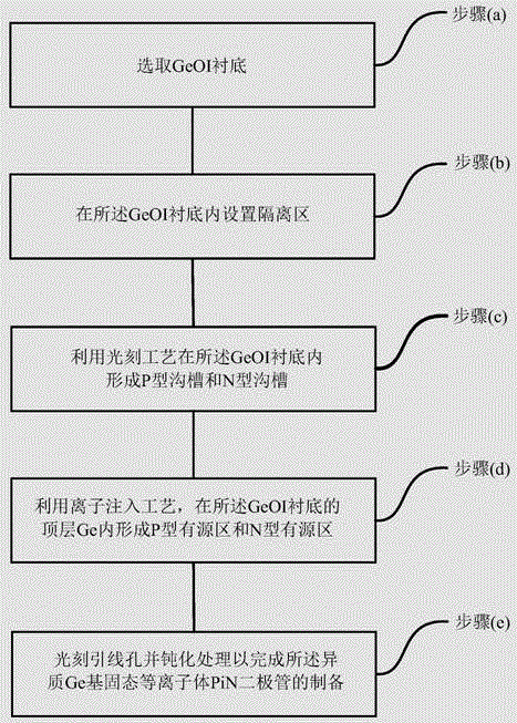
[0054] See figure 1 ,figure 1 It is a flow chart of a method for manufacturing a SiGe-Si-SiGe heterogeneous Ge-based solid-state plasma PiN diode according to an embodiment of the present invention. The method is suitable for preparing a GeOI-based lateral solid-state plasma PiN diode, and the GeOI lateral solid-state plasma PiN diode Bulk PiN diodes are mainly used to make solid-state plasmonic antennas. The method comprises the steps of:

[0055] (a) select a GeOI substrate;

[0056] (b) setting an isolation region in the GeOI substrate;

[0057] (c) forming a P-type trench and an N-type trench in the GeOI substrate by photolithography;

[0058] (d) using an ion implantation process to form a P-type active region and an N-type active region in the top layer Ge of the GeOI substrate;

[0059] (e) Lithographic lead holes and passivation treatment to complete the preparation of the heterogeneous Ge-based solid-state plasmonic PiN diode.

[0060] Among them, for step (a), t...

Embodiment 2

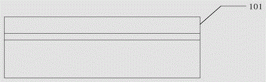
[0096] See Figure 2a-Figure 2r , Figure 2a-Figure 2r It is a schematic diagram of a method for preparing a SiGe-Si-SiGe heterogeneous Ge-based solid-state plasma PiN diode according to an embodiment of the present invention. On the basis of the above-mentioned embodiment 1, the length of the prepared channel is 22nm (the length of the solid-state plasma region is 100 nm. Micron) GeOI-based solid-state plasma PiN diode as an example to describe in detail, the specific steps are as follows:

[0097] Step 1, substrate material preparation steps:

[0098] (1a) if Figure 2a As shown, the (100) crystal orientation is selected, the doping type is p-type, and the doping concentration is 10 14 cm -3 A GeOI substrate sheet 101, the thickness of the top layer Ge is 50 μm;

[0099] (1b) if Figure 2b As shown, a first layer of SiO with a thickness of 40nm is deposited on a GeOI substrate by chemical vapor deposition (Chemical vapor deposition, CVD for short). 2 layer 201;

[01...

Embodiment 3

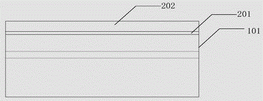
[0127] Please refer to image 3 , image 3 It is a schematic diagram of the device structure of a SiGe-Si-SiGe heterogeneous Ge-based solid-state plasma PiN diode according to an embodiment of the present invention. The heterogeneous Ge-based solid-state plasma PiN diode adopts the above-mentioned figure 1 The preparation method shown is made, specifically, the Ge-based solid-state plasma PiN diode is prepared and formed on the GeOI substrate 301, and the P region 304, the N region 305 of the PiN diode and the laterally located P region 304 and the N region The I regions between 305 are located in the top layer Ge302 of the GeOI substrate. Wherein, the PiN diode can be isolated by STI deep trenches, that is, an isolation trench 303 is provided outside the P region 304 and the N region 305, and the depth of the isolation trench 303 is greater than or equal to the thickness of the top layer Ge302.


PUM


Abstract

The invention relates to a preparation method and a device of a SiGe-Si-SiGe heterogeneous Ge-based solid-state plasma PiN diode. The preparation method comprises the steps of (a), selecting a GeOI substrate; (b), setting an isolation region in the GeOI substrate; (c), forming a P type trench and an N type trench in the GeOI substrate through a photoetching process; (d), adopting an ion implantation process to form a P type active region and an N type active region in top layer Ge of the GeOI substrate; and (e) performing lead hole photoetching and passivating treatment to complete the preparation of the heterogeneous Ge-based solid-state plasma PiN diode. According to the embodiments, the high-performance Ge-based solid-state plasma PiN diode, which is applicable to formation of a solid-state plasma antenna, can be prepared and provided through a deep trench isolation technology and the ion implantation process.

Description

technical field [0001] The invention relates to the technical field of semiconductor device manufacturing, in particular to a method for preparing a SiGe-Si-SiGe heterogeneous Ge-based solid-state plasma PiN diode and a device thereof. Background technique [0002] At present, the materials used in PiN diodes used in plasma reconfigurable antennas at home and abroad are all bulk silicon materials. This material has the problem of low carrier mobility in the intrinsic region, which affects the carrier concentration in the intrinsic region of the PiN diode, and then Affect its solid-state plasma concentration; and the P region and N region of this structure are mostly formed by implantation process, which requires a large implant dose and energy, high requirements on equipment, and is incompatible with existing processes; and the diffusion process, Although the junction depth is deep, the areas of the P region and the N region are large, the integration degree is low, and the ...

Claims


Application Information

Patent Timeline
IPC IPC(8): H01L21/329H01L29/868
CPCH01L29/6609H01L29/868
Inventor 王斌苏汉康海燕胡辉勇杨佳音张鹤鸣宋建军舒斌宣荣喜郝敏如
Owner 陕西天道必成信息技术有限责任公司
Why Eureka
Try Eureka