Back emitter junction back-surface tunnel oxidation and passivation contact efficient battery production method

A technology of tunnel oxidation and manufacturing method, which is applied in the direction of photovoltaic power generation, circuits, electrical components, etc., can solve the problems of electrical performance to be improved, and achieve the effect of easy production equipment and process, strong process feasibility, and easy compatibility

Inactive Publication Date: 2017-05-31
SHANGHAI SHENZHOU NEW ENERGY DEV
View PDF11 Cites 7 Cited by
  • Summary
  • Abstract
  • Description
  • Claims
  • Application Information

AI Technical Summary

Problems solved by technology

Although this patent solves the problem of the aluminum emitter junction leakage channel caused by the direct printing of the silver back busbar or the silver aluminum back busbar on the silicon wafer after sintering, there is still a problem that the electrical performance needs to be improved

Method used


Image

  • Back emitter junction back-surface tunnel oxidation and passivation contact efficient battery production method

Examples


Embodiment 1

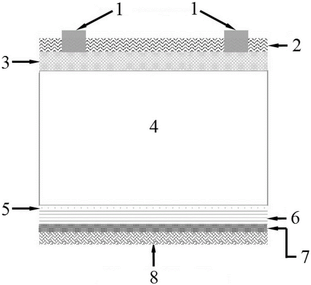
[0023] A method for fabricating a high-efficiency battery with back tunnel oxidation passivation contact at the back emitter junction adopts the following steps:

[0024] (1) Using the silicon chip in KOH alkali solution and H 2 o 2 Remove the damaged layer in the solution, then use tetramethylammonium hydroxide and isopropanol to form a mixed solution to texture the silicon wafer, and form a pyramid texture with 1 μm on both sides;

[0025] (2) Diffusion method is adopted on the front side of the silicon wafer to form N + front surface field;

[0026] (3) Use HF solution to remove borosilicate glass BSG layer, and use HNO 3 Mixed solution with HF for side insulation and back polishing;

[0027] (4) A layer of ultra-thin tunnel oxide layer SiO with a thickness less than 2nm is grown on the back of the silicon wafer by wet chemical method 2 , and then grow B-doped P with a thickness of 15nm on it by PECVD + Polysilicon layer, adopts fluorosilicate H in the present embodim...

Embodiment 2

[0033] A method for fabricating a high-efficiency battery with back tunnel oxidation passivation contact at the back emitter junction adopts the following steps:

[0034] (1) Using the silicon chip in NaOH alkali solution and H 2 o 2 Remove the damaged layer in the solution, then use tetramethylammonium hydroxide and isopropanol to form a mixed solution to texture the silicon wafer, and form a pyramid texture with 2 μm on both sides;

[0035] (2) The method of ion implantation is adopted on the front side of the silicon wafer to form N + front surface field;

[0036] (3) Use HF solution to remove borosilicate glass BSG layer, and use HNO 3 Mixed solution with HF for side insulation and back polishing;

[0037] (4) A layer of ultra-thin tunnel oxide layer SiO with a thickness less than 2nm is grown on the back of the silicon wafer by wet chemical method 2 , and then grow B-doped P with a thickness of 18nm on it by PECVD + Polysilicon layer; take fluorosilicate H 2 SiO 6...

Embodiment 3

[0042] A method for fabricating a high-efficiency battery with back tunnel oxidation passivation contact at the back emitter junction adopts the following steps:

[0043] (1) Using the silicon chip in NaOH alkali solution and H 2 o 2 Remove the damaged layer in the solution, then use tetramethylammonium hydroxide and isopropanol to form a mixed solution to texture the silicon wafer, and form a pyramid texture with 4 μm on both sides;

[0044] (2) The method of ion implantation is adopted on the front side of the silicon wafer to form N + front surface field;

[0045] (3) Use HF solution to remove borosilicate glass BSG layer, and use HNO 3 Mixed solution with HF for side insulation and back polishing;

[0046] (4) A layer of ultra-thin tunnel oxide layer SiO with a thickness less than 2nm is grown on the back of the silicon wafer by wet chemical method 2 , and then grow B-doped P with a thickness of 20nm on it by PECVD + polysilicon layer; we take fluorosilicate H 2 SiO...


PUM


Abstract

The invention relates to a back emitter junction back-surface tunnel oxidation and passivation contact efficient battery production method, comprising: removing the damage layer of a silicon wafer and making velvets; and then performing edge insulation and back polishing; growing an ultra-thin tunnel oxide layer SiO2 on the back of the silicon wafer; using the PECVD method or other CVD methods to grow a B-doped polysilicon layer on the ultra-thin tunnel oxide layer SiO2; depositing an aluminum oxide layer on the surface of the B-doped polysilicon layer; growing a hydrogenated amorphous silicon nitride passivation antireflective layer on the front surface of the silicon wafer; and finally, printing Ag slurry on the front surface of the silicon wafer to form an all-aluminum back-field A1-BSF structure at the back surface. Compared with the prior art, the method could replace the N type back emitter crystalline silicon battery back point contact mechanism through the utilization of an ultra-thin tunnel oxide layer SiO2 and a B-doped polysilicon layer. Such a composed layer could greatly reduce the composition of the back surface metal and the semiconductor surface.

Description

technical field [0001] The invention relates to a manufacturing method of a crystalline silicon cell, in particular to a manufacturing method of a high-efficiency cell with a rear emitter junction, rear tunnel oxidation passivation contact. Background technique [0002] The difference between back-emitter junction back tunnel oxidation passivation contact cell and conventional battery technology is the preparation of the composite structure of back tunnel oxidation passivation layer and doped polysilicon layer. The key point of this method is the ultra-thin tunnel Preparation control of the through-oxide layer and treatment of the interface state with the silicon substrate before preparation. Chinese patent CN203312314U discloses an N-type crystalline silicon solar cell that fully covers the aluminum back emitter junction, including a single crystal or polycrystalline silicon wafer, and a silver positive electrode printed on it, and an aluminum back main grid line is printed...

Claims


Application Information

Patent Timeline
Patent Type & Authority Applications(China)
IPC IPC(8): H01L31/18H01L31/068H01L31/0224
CPCH01L31/022441H01L31/02363H01L31/0682H01L31/1804Y02E10/547Y02P70/50
Inventor 汪建强钱峥毅郑飞林佳继张忠卫石磊阮忠立
Owner SHANGHAI SHENZHOU NEW ENERGY DEV
Why Eureka
Try Eureka