Making method of semiconductor chip
A manufacturing method and semiconductor technology, applied in semiconductor devices, electrical components, circuits, etc., can solve the problem of low external quantum efficiency of GaN-based LEDs, and achieve the effects of easy mass production, improved quantum efficiency, and improved luminous brightness.
- Summary
- Abstract
- Description
- Claims
- Application Information
AI Technical Summary
Problems solved by technology
Method used
Image
Examples
Embodiment 1
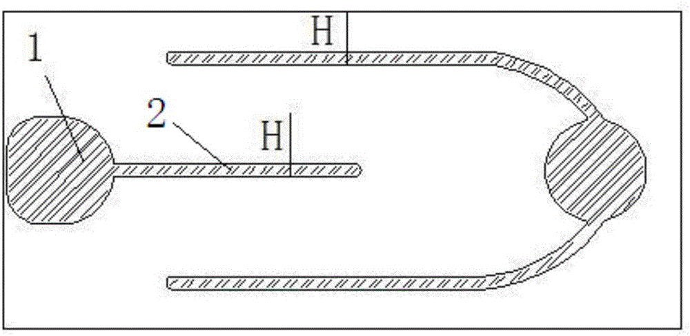
[0032] Grow a GaN epitaxial layer on a sapphire substrate, the thickness of the epitaxial layer is 6μm, and use an electron beam evaporation machine to evaporate a layer Thick ITO conductive expansion layer, followed by photolithography process to expose excess conductive expansion layer, with FeCl 3 Wet-etch the exposed conductive extension layer with a mixed solution of HCl, etch the epitaxial wafer with an ICP etching machine to expose the steps and the N-type GaN layer, the etching depth is 1.3-1.5 μm, and make a P-type electrode on the conductive extension layer , N-type electrode 1 is made on N-type GaN, the width H of N-type electrode line 2 is 10 μm, and then SiO is deposited by PECVD 2 Make a passivation layer, then test the adhesion between the metal electrode and the conductive extension layer, and then complete the post-processing steps such as wafer thinning, back-plating reflective layer, cutting slivers, point measurement and sorting, etc. The luminous brightn...
Embodiment 2
[0034] Grow a GaN epitaxial layer on a sapphire substrate, the thickness of the epitaxial layer is 6μm, and use an electron beam evaporation machine to evaporate a layer Thick ITO conductive expansion layer, followed by photolithography process to expose excess conductive expansion layer, with FeCl 3 Wet-etch the exposed conductive extension layer with a mixed solution of HCl, etch the epitaxial wafer with an ICP etching machine to expose the steps and the N-type GaN layer, the etching depth is 1.3-1.5 μm, and make a P-type electrode on the conductive extension layer , make N-type electrodes on N-type GaN, the electrode line width is 7μm, and then use PECVD to deposit SiO 2 Make a passivation layer, then test the adhesion between the metal electrode and the conductive extension layer, and then complete the post-processing steps such as wafer thinning, back-plating reflective layer, cutting slivers, point measurement and sorting, etc. The luminous brightness of the 150mA test...
Embodiment 3
[0036] Grow a GaN epitaxial layer on a sapphire substrate, the thickness of the epitaxial layer is 6μm, and use an electron beam evaporation machine to evaporate a layer Thick ITO conductive expansion layer, followed by photolithography process to expose excess conductive expansion layer, with FeCl 3 Wet-etch the exposed conductive extension layer with a mixed solution of HCl, etch the epitaxial wafer with an ICP etching machine to expose the steps and the N-type GaN layer, the etching depth is 1.3-1.5 μm, and make a P-type electrode on the conductive extension layer , make N-type electrodes on N-type GaN, the electrode line width is 5 μm, and then use PECVD to deposit SiO 2 Make a passivation layer, then test the adhesion between the metal electrode and the conductive extension layer, and then complete the post-processing steps such as wafer thinning, back-plating reflective layer, cutting slivers, point measurement and sorting, etc. The luminous brightness of the 150mA tes...
PUM
| Property | Measurement | Unit |
|---|---|---|
| width | aaaaa | aaaaa |
| width | aaaaa | aaaaa |
| thickness | aaaaa | aaaaa |
Abstract
Description
Claims
Application Information
