Ultra-wideband absorption heterojunction solar cell
A solar cell and heterojunction technology, applied in circuits, photovoltaic power generation, electrical components, etc., can solve the problems of low light absorption efficiency in the visible light band and unusable light energy, and achieve the effect of improving photoelectric conversion efficiency
- Summary
- Abstract
- Description
- Claims
- Application Information
AI Technical Summary
Problems solved by technology
Method used
Image
Examples
example example 1
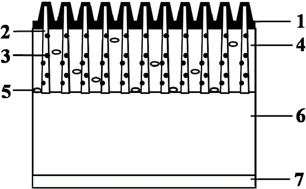
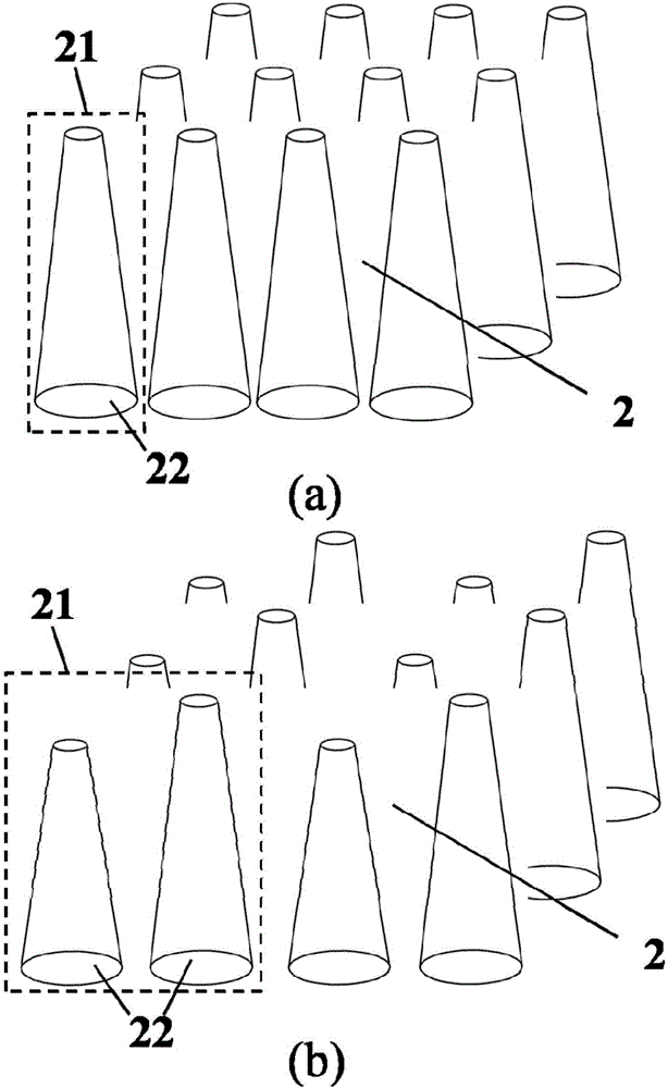
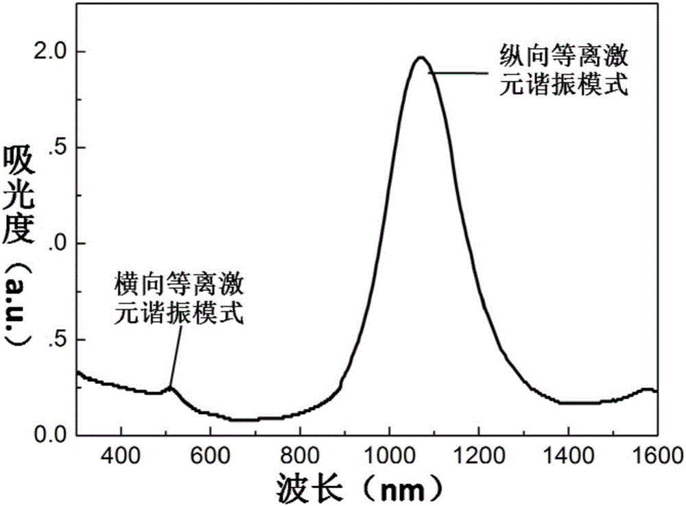
[0038] In the battery structure, the nanocone unit structure has only one nanocone with structural parameters (such as figure 2 a), the spacing is 50 nanometers, the material of the nanocone is gold, the width of the tip is 15 nanometers, the width of the bottom is 15 nanometers, and the height is 100 nanometers. The transverse plasmon resonance absorption and longitudinal plasmon absorption spectra are as follows image 3 As shown, its transverse plasmon resonance absorption peak is located at about 520 nanometers, and its longitudinal plasmon resonance absorption peak is located at about 1100 nanometers; the material of the transparent conductive front electrode is indium tin oxide ITO with a thickness of 100 nanometers; the down-conversion quantum The dot material is cadmium selenide quantum dot material; the organic conductive polymer layer material is poly 3,4-ethylenedioxythiophene-polystyrene sulfonic acid PEDOT:PSS, with a thickness of 70 nanometers; the plasmonic ligh...
example example 2
[0040] In the battery structure, the nanocone unit structure has two kinds of nanocones with structural parameters, and the arrangement of the three nanocones is as follows: figure 2 As shown in b, the material of the nanocone is silver, the width of the tip is 10 nanometers, the width of the bottom is 15 nanometers, and the height is 120 nanometers and 140 nanometers respectively. The distance between different nanocones in the unit structure is 50 nanometers, and the distance between the nanocone array units is 130 nanometers ; down-converting nanostructures to samarium Sm 3+ Doped with quantum dot materials; the material of the transparent conductive front electrode is aluminum-doped zinc oxide AZO, with a thickness of 120 nanometers; the material of the organic conductive polymer layer is poly-3-octylthiophene P3OT, with a thickness of 80 nanometers; plasmonic light trapping The palladium decahedron is selected as the structure, and the size is 40 nanometers; the semicond...
PUM
 Abstract
Description
Claims
Application Information
 - R&D
- Intellectual Property
- Life Sciences
- Materials
- Tech Scout
- Unparalleled Data Quality
- Higher Quality Content
- 60% Fewer Hallucinations
Browse by: Latest US Patents, China's latest patents, Technical Efficacy Thesaurus, Application Domain, Technology Topic, Popular Technical Reports.
© 2025 PatSnap. All rights reserved.Legal|Privacy policy|Modern Slavery Act Transparency Statement|Sitemap|About US| Contact US: help@patsnap.com


