A high power density substrate embedded with diamond copper and its preparation method

A high power density, diamond technology, used in metal processing equipment, welding equipment, manufacturing tools, etc., can solve the problems of high price, low thermal conductivity, high relative density, etc., to save raw materials, high thermal conductivity, high density small effect

Active Publication Date: 2018-10-02
GRIMAT ENG INST CO LTD
View PDF6 Cites 0 Cited by
  • Summary
  • Abstract
  • Description
  • Claims
  • Application Information

AI Technical Summary

Problems solved by technology

[0006] Aiming at the problems of low thermal conductivity, high relative density and high price in current electronic packaging materials, the present invention proposes a high power density substrate embedded with diamond copper and a preparation method thereof

Method used


Image

  • A high power density substrate embedded with diamond copper and its preparation method
  • A high power density substrate embedded with diamond copper and its preparation method
  • A high power density substrate embedded with diamond copper and its preparation method

Examples


Embodiment 1

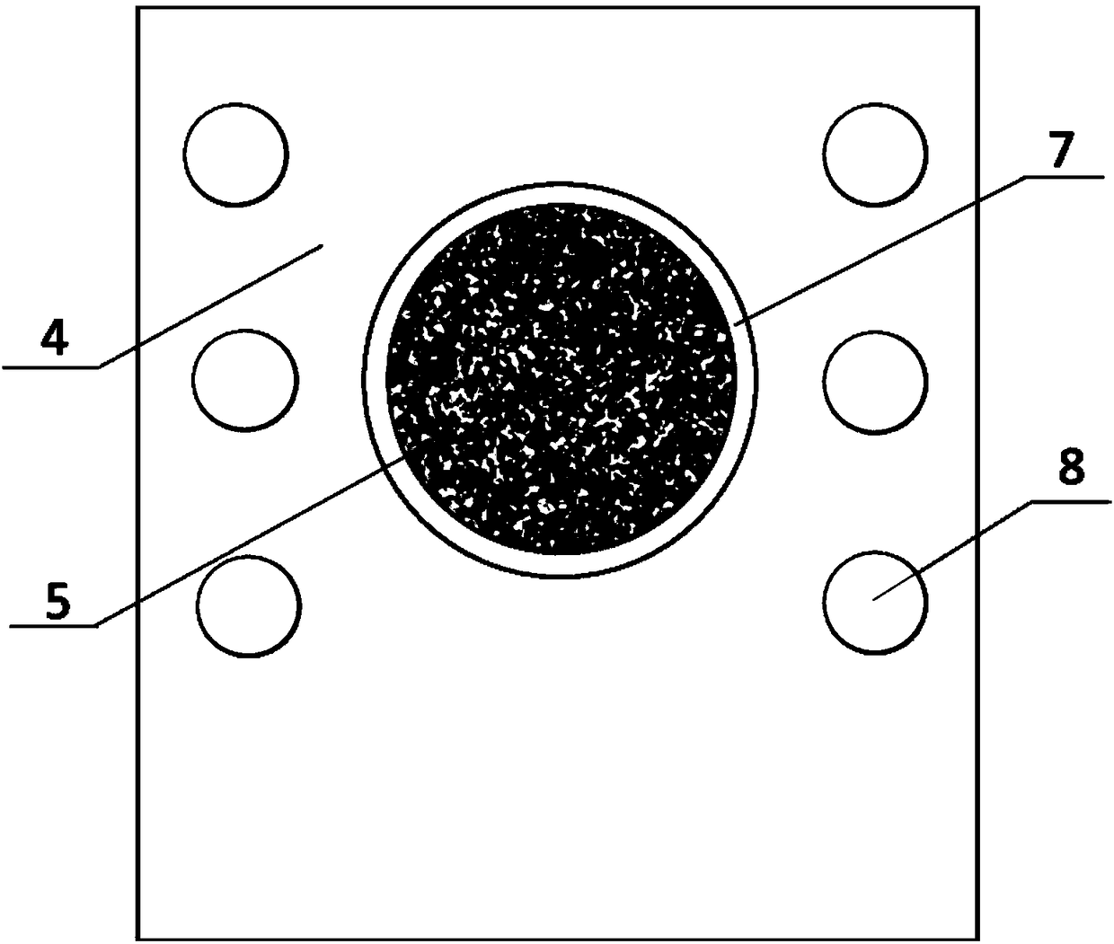
[0024] combine figure 1 and figure 2 To illustrate this example, a porous diamond preform is placed at position 2 of the near-net mold, and a high-power-density substrate with 5×20 mm rectangular diamond / copper embedded in oxygen-free copper is prepared by vacuum pressure infiltration technology, and the thermal load power is applied 400W / cm 2 , The junction temperature of the chip tested by a thermal imager is 56°C, which is 8-10°C lower than the junction temperature of the oxygen-free copper substrate.

Embodiment 2

[0026] combine figure 1 and figure 2 To illustrate this example, a porous diamond preform is placed at position 2 of the near-net mold, and a high power density substrate with 8×30mm rectangular diamond / copper embedded in oxygen-free copper is prepared by vacuum pressure infiltration technology, and the thermal load power is applied 600W / cm 2 , The junction temperature of the chip tested by a thermal imager is 63°C, which is 20-25°C lower than the junction temperature of the oxygen-free copper metal substrate.

Embodiment 3

[0028] combine figure 1 and figure 2 To illustrate this embodiment, first add molybdenum powder to position 1 of the near-net shape mold and then sinter it into porous molybdenum, fill diamond powder at position 2 of the near-net shape mold, and sinter again to obtain a composite porous preform inlaid with diamonds, using vacuum pressure The high power density substrate of 8×30mm rectangular diamond / copper embedded in molybdenum copper was prepared by impregnation technology, and the applied thermal load power was 400W / cm 2 , The junction temperature of the chip tested by a thermal imager is 64°C, which is 18-20°C lower than the junction temperature of the molybdenum-copper metal substrate.


PUM


Abstract

The invention provides a high power density substrate embedded with diamond copper and a preparation method thereof. The substrate body includes a diamond copper composite material part and a tungsten copper, molybdenum copper alloy or oxygen-free copper part. The alloy part is inlaid on the composite material or the composite material is inlaid on the alloy, the two parts are metallurgically bonded or welded together, and the vacuum pressure impregnation process can be used to directly form near-finish. The substrate has a higher thermal conductivity than alloy materials such as tungsten copper; the thermal expansion coefficient matches that of semiconductor materials; it is easy to machine and has better machinability than pure diamond copper materials; the relative mass is small and the price is moderate, which is convenient for popularization and use , can meet the heat dissipation requirements of high-power electronic devices, and solve the heat dissipation problem that restricts the development of electronic devices to high power and miniaturization.

Description

technical field [0001] The invention belongs to the technical field of electronic packaging, in particular to a high power density substrate embedded with diamond copper and a preparation method thereof. Background technique [0002] With the rapid development of microelectronics technology, the third-generation wide-bandgap semiconductor chips represented by GaN chips have begun to be widely used, and the control of the heat of electronic devices has become the key to their normal operation, which puts forward higher requirements for electronic packaging materials. . An ideal electronic packaging material should have high thermal conductivity, a thermal expansion coefficient that matches chips such as GaN, and certain strength and rigidity. [0003] At present, tungsten-copper and molybdenum-copper alloys are widely used in the market, and their thermal conductivity is up to 280W / mK, which can no longer meet the heat dissipation requirements of high-power chips. In additio...

Claims


Application Information

Patent Timeline
Patent Type & Authority Patents(China)
IPC IPC(8): C22C1/10B23K1/00B23K101/36
CPCC22C1/1015C22C1/1036B23K1/00B23K2101/36C22C1/1073
Inventor 郭宏张习敏王亚宝刘铭坤
Owner GRIMAT ENG INST CO LTD
Why Eureka
Try Eureka