A kind of blue organic electroluminescence device and preparation method thereof

A luminescent, blue technology, applied in the field of blue organic electroluminescent devices and its preparation, can solve the problem that the comprehensive performance of pure blue organic electroluminescent devices has not been substantially improved in terms of color purity, luminous efficiency and work stability , reduce the stability of the device, the low power efficiency of the device and other issues

Active Publication Date: 2019-02-12
CHANGCHUN INST OF APPLIED CHEMISTRY - CHINESE ACAD OF SCI
View PDF2 Cites 0 Cited by
  • Summary
  • Abstract
  • Description
  • Claims
  • Application Information

AI Technical Summary

Problems solved by technology

Although the color purity and color stability of the obtained dark blue device are excellent, its high operating voltage not only directly leads to the low power efficiency of the device, but also indirectly reduces the working stability of the device.
It can be seen that the overall performance of pure blue organic electroluminescent devices such as color purity, luminous efficiency and working stability has not been substantially improved.

Method used


Image

  • A kind of blue organic electroluminescence device and preparation method thereof
  • A kind of blue organic electroluminescence device and preparation method thereof
  • A kind of blue organic electroluminescence device and preparation method thereof

Examples


preparation example Construction

[0049] The present invention also provides a method for preparing the above-mentioned blue organic electroluminescent device, comprising the following steps:

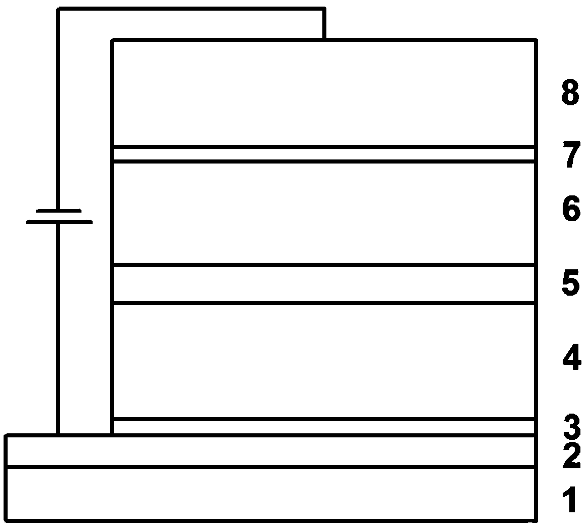
[0050] forming an anode layer on the substrate;

[0051] A light-emitting layer is formed on the anode layer; the light-emitting layer is formed by a blue organic fluorescent material and a hole-type organic host material; the mass of the blue organic fluorescent material is 8.0% to 8.0% of the mass of the hole-type organic host material 25.0%; the excited state energy of the blue organic fluorescent material is less than the excited state energy of the hole-type organic host material;

[0052] A cathode is formed on the light-emitting layer to obtain a blue organic electroluminescent device.

[0053] According to the present invention, the anode layer is first formed on the substrate; the substrate and the anode layer are the same as those described above, and will not be repeated here. In the present invention, it i...

Embodiment 1

[0065] First, the ITO anode layer on the ITO glass is laser-etched to form a patterned electrode, and then ultrasonically cleaned with cleaning solution and deionized water for 15 minutes and dried in an oven. Then put the dried substrate into the pretreatment vacuum chamber, and then transfer the ITO anode to the metal evaporation chamber after a 10-minute low-pressure oxygen plasma treatment with a voltage of 400 volts in an atmosphere with a vacuum degree of 10 Pa. In 3~5×10 -5 Evaporation of 3nm MoO in a vacuum atmosphere of Pa 3 Anode interface layer 3. Then, the unfinished device was transferred to an organic evaporation chamber at a vacuum of 1-3×10 -5 Under the vacuum atmosphere of Pascal, on the anode interface layer 3, vapor-deposit 40 nanometer thick TAPC hole transport layer / electron blocking layer 4, 10 nanometer thick DBzA doped TcTa light emitting layer 5, 40 nanometer thick TmPyPB hole blocking layer layer / electron transport layer6. Next, the unfinished dev...

Embodiment 2

[0071] First, the ITO anode layer on the ITO glass is laser-etched to form a patterned electrode, and then ultrasonically cleaned with cleaning solution and deionized water for 15 minutes and dried in an oven. Then put the dried substrate into the pretreatment vacuum chamber, and then transfer the ITO anode to the metal evaporation chamber after a 10-minute low-pressure oxygen plasma treatment with a voltage of 400 volts in an atmosphere with a vacuum degree of 10 Pa. In 3~5×10 -5 Evaporation of 3nm MoO in a vacuum atmosphere of Pa 3 Anode interface layer 3. Then, the unfinished device was transferred to an organic evaporation chamber at a vacuum of 1-3×10 -5 Under the vacuum atmosphere of Pascal, on the anode interface layer 3, 40 nanometer thick TAPC hole transport layer / electron blocking layer 4, 10 nanometer thick DBzA doped TcTa light emitting layer 5, 40 nanometer thick Tm3PyP26PyB hole blocking layer were sequentially evaporated. layer / electron transport layer6. Nex...


PUM


Abstract

The invention provides a blue organic electroluminescent device, comprising: a substrate; an anode layer arranged on the substrate; a light emitting layer arranged on the anode layer; the light emitting layer is composed of blue organic fluorescent The material is formed with a hole-type organic host material; the mass of the blue organic fluorescent material is 8.0% to 25.0% of the mass of the hole-type organic host material; and a cathode layer arranged on the light-emitting layer. Compared with the prior art, the present invention adopts the blue organic fluorescent material whose excited state energy is smaller than that of the hole-type organic host material as the luminescent material, which has both high luminous efficiency and color purity, good thermal stability, and superior Electron transport ability, high doping concentration in the light-emitting layer, can have both the functions of the host material and the blue light material, which is conducive to balancing the distribution of holes and electrons in the light-emitting region, and can also limit the recombination of holes and electrons in the light-emitting area The narrow area of ​​the layer can effectively balance the distribution of carriers in the light-emitting layer.

Description

technical field [0001] The invention belongs to the technical field of organic electroluminescence, and in particular relates to a blue organic electroluminescence device and a preparation method thereof. Background technique [0002] An organic light emitting device is a self-luminous device, and when charges are injected into an organic film between an electron injection electrode (anode) and a hole injection electrode (cathode), electrons and holes are combined and then annihilated, thereby generating light. Compared with other flat display technologies such as liquid crystal displays, plasma display devices, and field emission displays, organic electroluminescent displays have the advantages of adjustable luminous color, active luminescence, high brightness, high efficiency, wide viewing angle, low energy consumption, simple preparation process, It can produce a series of excellent characteristics such as curved and flexible display screens, and has broad application pro...

Claims


Application Information

Patent Timeline
Patent Type & Authority Patents(China)
IPC IPC(8): H01L51/50H01L51/54H01L51/56
CPCH10K85/615H10K50/12H10K71/00H10K85/657H10K50/11H10K2101/40
Inventor 周亮张洪杰赵学森
Owner CHANGCHUN INST OF APPLIED CHEMISTRY - CHINESE ACAD OF SCI
Why Eureka
Try Eureka