Method for growing alternating polarity GaN structure on Ga-polar GaN template

A technology of growing polarity and polarity, which is applied in the direction of electrical components, semiconductor/solid-state device manufacturing, circuits, etc., can solve the problems of high cost of GaN substrate and difficult popularization of GaN structure, so as to save etching steps, crystal High quality and avoid damage effect

Inactive Publication Date: 2017-06-13
UNIV OF SCI & TECH BEIJING
View PDF4 Cites 2 Cited by
  • Summary
  • Abstract
  • Description
  • Claims
  • Application Information

AI Technical Summary

Problems solved by technology

At present, although the use of HVPE and ammonothermal method to prepare GaN bulk materials is becoming more and more mature, the cost of GaN substrates is still high, and it is still difficult to popularize GaN structures with periodic growth orientation and thicker GaN structures.

Method used


Image

  • Method for growing alternating polarity GaN structure on Ga-polar GaN template
  • Method for growing alternating polarity GaN structure on Ga-polar GaN template
  • Method for growing alternating polarity GaN structure on Ga-polar GaN template

Examples


Embodiment 1

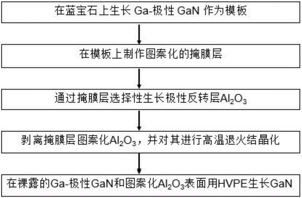
[0044] Methods for growing alternating N- and Ga-polar GaN structures on sapphire substrates:

[0045] Step 1: Clean the sapphire substrate with isopropanol, acetone, methanol, alcohol, and deionized water at room temperature for 5 minutes, and finally wash it with N 2 blow dry.

[0046] Step 2: Put the cleaned sapphire substrate in the MOCVD reaction chamber, using triethylgallium TEG and NH 3 As a source, Ga-polar GaN with a film thickness of 1.5-2um is grown under conditions of a temperature of 1100°C, a chamber pressure of 150Torr, and a V / III ratio of 600-3000. ;

[0047] Step 3: Using the Ga-polar GaN layer as a template, prepare a patterned mask layer PVP: soak the above sample in deionized water for 2 minutes, and then use 80°C standard cleaning solution SC1 (NH 4 0H:H 2 o 2 :H 2 (O=1:1:5) wash for 10 minutes, then wash with deionized water and blow dry with nitrogen, then spin-coat PVP with a thickness between 0.1-1um on a glue coater, and then put it in an oven...

Embodiment 2

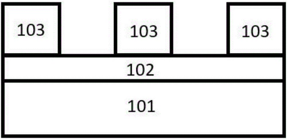
[0052] 1) Refer to figure 2 , the sapphire substrate 101 was ultrasonically cleaned with isopropanol, acetone, methanol, and alcohol at room temperature for 5 minutes, then repeatedly rinsed with deionized water, and washed with N 2 blow dry. Place the cleaned sapphire substrate 101 in the MOCVD reaction chamber, using triethylgallium TEG and NH 3 As a source material, a 2um Ga-polar GaN layer 102 was grown under conditions of a temperature of 1100° C., a chamber pressure of 150 Torr, and a V / III ratio of 3000.

[0053] 2) Refer to image 3 , using the Ga-polar GaN layer 102 as a template to prepare a patterned mask layer PVP 103: first soak the sample in the previous step in deionized water for 2 minutes, and then use 80°C standard cleaning solution SC1 (NH40H: H2O2:H2O=1:1:5) for 10 minutes, then rinsed with deionized water and blown dry with nitrogen, then put PVP with a thickness of 100nm on a glue coater, and then baked in an oven at 100°C for 60 Minutes, the dried P...


PUM

PropertyMeasurementUnit
thicknessaaaaaaaaaa

Abstract

The invention provides a method for growing alternating polarity GaN structure on a Ga-polar GaN template and belongs to the field of semiconductor technologies and devices. Ga-polar GaN growing on a sapphire substrate through MOCVD serves as the template, a patterned polyvinylpyrrolidone film is manufactured on the template through the photoetching technology to serve as a mask layer, Al2O3 used for polarity inversion selectively grows on the mask layer by means of the PE-ALD method, the PE-ALD method can make the process temperature lower than the melting point of the mask layer, a Al2O3 thin film which is good in uniformity and whose thickness can be precisely controlled can be prepared while it is guaranteed that the mask layer does not deform, the patterned Al2O3 of the mask layer is stripped and subjected to crystallization through high-temperature annealing, finally, thick film GaN growth is conducted on the exposed Ga-polar GaN template and the patterned Al2O3 through the hydride vapor phase epitaxy method, and the alternating polarity GaN requirement that the thickness of a high-power device needs to reach 1 mm is hopeful to be met.

Description

technical field [0001] The invention relates to the field of semiconductor technology and devices, in particular to a method for growing a GaN structure with alternating polarity on a Ga-polar GaN template. Background technique [0002] Wurtzite-structured GaN has a hexagonal crystal structure, and the positive and negative charges in the C-axis direction are not centrosymmetric, and have an intrinsic polarization effect. In the bonding of N and Ga, the covalent bond electrons are biased towards N, so the spontaneous pole The direction of transformation is N to Ga, and it is Ga to N in the +C(0001) direction, showing Ga-polarity, and Ga-polarity in the -C(000-1) direction, and they have significantly different characteristics. Such as chemical activity, doping efficiency, polarization direction, work function, surface morphology and internal electric field, etc. Although hexagonal GaN semiconductors have such different polarities, current GaN-based devices still basically a...

Claims


Application Information

Patent Timeline
Patent Type & Authority Applications(China)
IPC IPC(8): H01L21/02
CPCH01L21/0242H01L21/02178H01L21/02271H01L21/02318H01L21/02458H01L21/0254H01L21/0262
Inventor 刘三姐郑新和彭铭曾侯彩霞王瑾何荧峰李美玲
Owner UNIV OF SCI & TECH BEIJING
Why Eureka
Try Eureka