Electrode lead unit, vacuum optoelectronic device and manufacturing method thereof

An electrode lead and manufacturing method technology, applied in the field of optoelectronic devices, can solve problems such as the inability to meet the needs of multi-electrode leads, and achieve the effects of avoiding device explosion or slow gas leakage, reliable performance, and easy mass production.

Active Publication Date: 2018-05-29
XI'AN INST OF OPTICS & FINE MECHANICS - CHINESE ACAD OF SCI
View PDF9 Cites 0 Cited by
  • Summary
  • Abstract
  • Description
  • Claims
  • Application Information

AI Technical Summary

Problems solved by technology

[0012] In order to solve the technical problem that the existing vacuum optoelectronic device manufacturing method cannot meet the requirements of multi-electrode leads, the present invention provides an electrode lead unit, a vacuum optoelectronic device and a manufacturing method thereof

Method used


Image

  • Electrode lead unit, vacuum optoelectronic device and manufacturing method thereof
  • Electrode lead unit, vacuum optoelectronic device and manufacturing method thereof
  • Electrode lead unit, vacuum optoelectronic device and manufacturing method thereof

Examples


Embodiment Construction

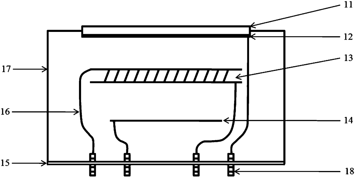
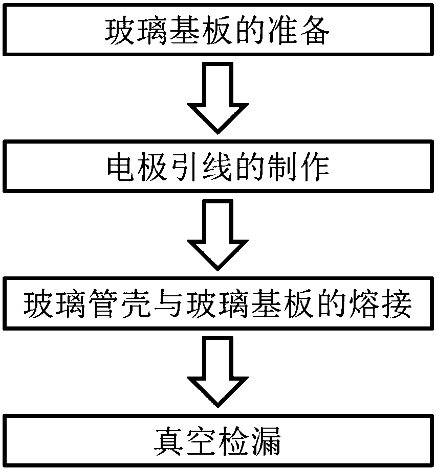
[0052] see figure 2 , the preferred implementation method of the present invention to make the electrode lead unit mainly includes the following steps:

[0053] First, the preparation of the glass substrate. Usually the glass substrate is made of borosilicate glass with a thickness of 2 mm and a flat surface. The size of the glass substrate is larger than 20 mm × 20 mm. It is ultrasonically cleaned with a glass cleaner and dried at high temperature.

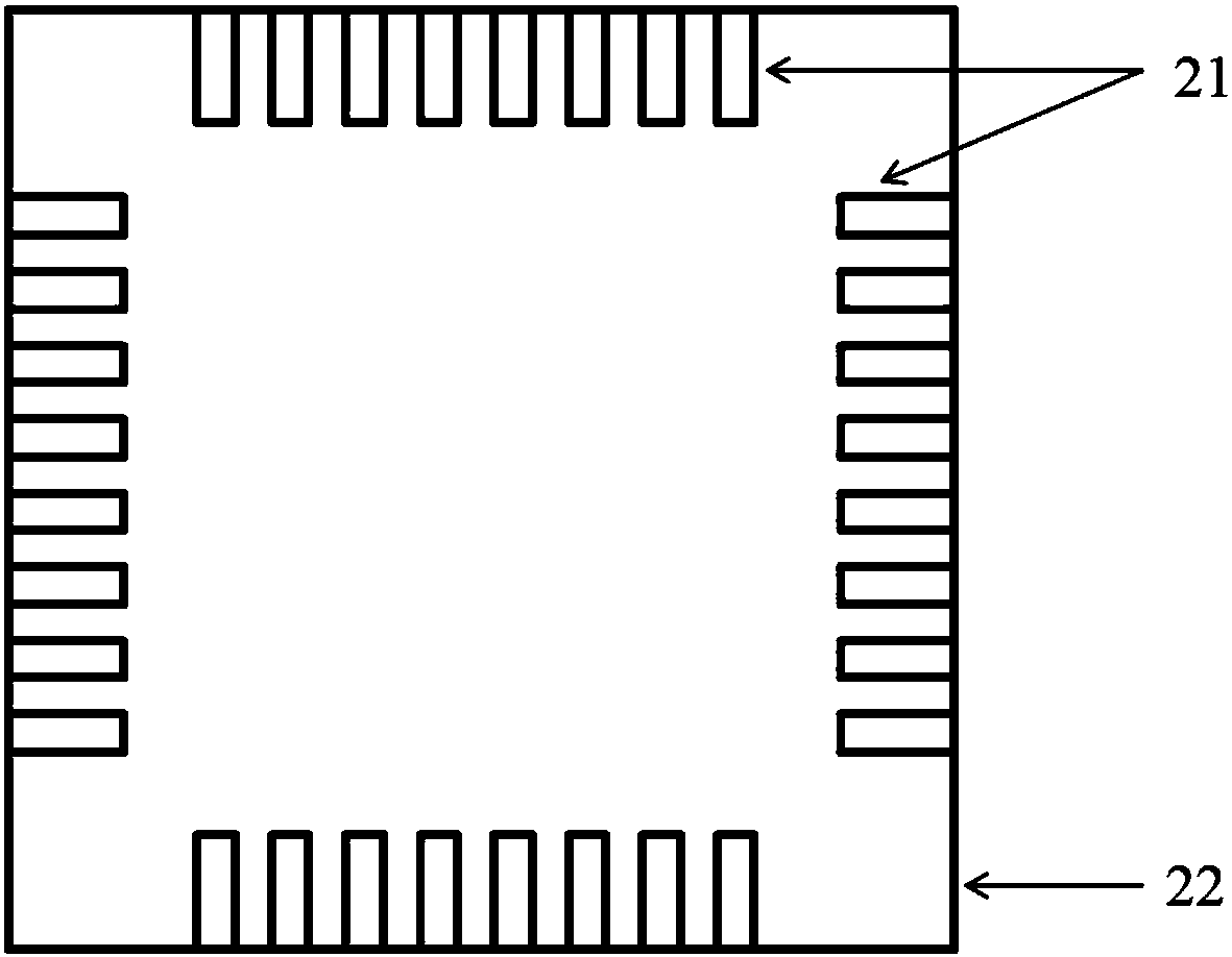
[0054] Second, the fabrication of electrode leads. Electrode leads are fabricated on glass substrates using standard semiconductor processes. The standard semiconductor process includes metal film deposition, photolithography, etching or corrosion or peeling, etc. The metal film can choose a single metal such as gold, silver or a stacked structure of multiple metal films such as titanium and platinum. The thickness of the metal film is greater than 500 nanometers. image 3 It is a typical electrode lead distribution state for...


PUM


Abstract

The invention belongs to the technical field of photoelectric devices, and relates to an electrode lead unit, a vacuum photoelectric device and a manufacturing method thereof. The electrode lead unit comprises a glass substrate, a glass package and multiple electrode leads; the glass package is welded on the surface of the glass substrate; the electrode leads are distributed on the welding surface between the glass package and the glass substrate; and one end of each electrode lead is located at the inner side of the glass package, and the other end of the electrode lead is located at the outer side of the glass package. Due to the manufactured electrode lead unit and no limitation from the diameter of a Kovar alloy wire at the tail end of an anode, a vacuum photoelectric device with hundreds of readout channels can be manufactured. The size of the electrode can reach tens of microns minimally, manufacturing of a high-density electrode lead can be realized, the electrode can be applied to multiple vacuum photoelectric devices such as a hybrid photodetector and a multi-anode photomultiplier tube, and has a wide application prospect in multiple fields such as high-energy physics, cosmic exploration, low light level night vision, and medical instruments.

Description

technical field [0001] The invention belongs to the technical field of photoelectric devices, and relates to an electrode lead unit, a vacuum photoelectric device and a manufacturing method thereof. Background technique [0002] Due to its excellent performance, such as high sensitivity, fast time response, large effective area, low dark current and excellent environmental adaptability, vacuum optoelectronic devices are widely used in high-energy physics, astrophysics, medical equipment, laser radar, low-light night vision, It has important applications in many fields such as environmental monitoring and plasma diagnosis, and is an important branch of photodetection devices. [0003] Vacuum optoelectronic devices are mainly composed of incident window, photocathode, electron optical system, electron multiplier and anode. Among them, the photocathode is attached to the incident window to convert the incident optical signal into an electrical signal; the electron optical syst...

Claims


Application Information

Patent Timeline
Patent Type & Authority Patents(China)
IPC IPC(8): H01J9/32H01J37/04H01J37/248H01J37/32H01J43/06
CPCH01J9/32H01J37/04H01J37/248H01J37/32532H01J43/06
Inventor 王兴田进寿
Owner XI'AN INST OF OPTICS & FINE MECHANICS - CHINESE ACAD OF SCI
Why Eureka
Try Eureka