Colorful solar cell and preparation method thereof

A solar cell, colorful technology, applied in circuits, photovoltaic power generation, electrical components, etc., can solve the problems of inability to reduce costs, high prices, and difficulty in reducing product manufacturing costs, and achieve low manufacturing costs, reasonable structure, and simple preparation methods. Effect

Active Publication Date: 2017-06-20
HEFEI INSTITUTES OF PHYSICAL SCIENCE - CHINESE ACAD OF SCI
View PDF4 Cites 0 Cited by
  • Summary
  • Abstract
  • Description
  • Claims
  • Application Information

AI Technical Summary

Problems solved by technology

Although this product can be used as a colored solar cell, it has shortcomings with its preparation method. First, the price of fluoride and yttrium oxide in the product is on the high side, w

Method used


Image

  • Colorful solar cell and preparation method thereof
  • Colorful solar cell and preparation method thereof

Examples


Embodiment 1

[0035] The concrete steps of preparation are:

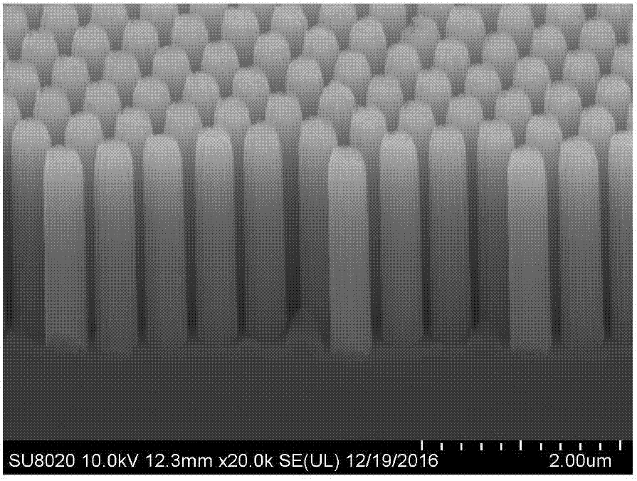
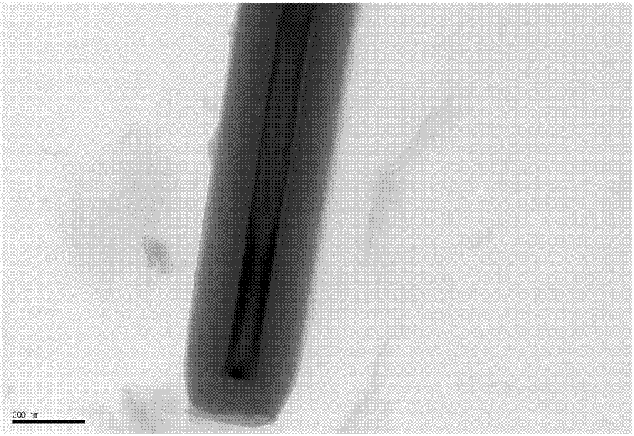
[0036] Step 1, using the nanosphere template method to make an ordered mask on the surface of the silicon substrate; wherein, the silicon substrate is a single crystal silicon substrate, and the process of using the nanosphere template method to make an ordered mask is to make a single layer dense After the row of polystyrene colloidal nanospheres with a diameter of 500nm is transferred to the surface of the silicon substrate, the diameter of the nanospheres is reduced to 50nm. A gold film with a thickness of 20 nm was evaporated on the surface to obtain a silicon substrate covered with an ordered gold mask. Then use a wet process to etch an ordered nanowire array on the silicon substrate covered with an ordered gold mask; wherein, the process of using a wet process to etch an ordered nanowire array is to cover the surface with The silicon substrate of the ordered gold mask was placed in 15 vol% hydrofluoric acid aqueous solutio...

Embodiment 2

[0040] The concrete steps of preparation are:

[0041] Step 1, using the nanosphere template method to make an ordered mask on the surface of the silicon substrate; wherein, the silicon substrate is a single crystal silicon substrate, and the process of using the nanosphere template method to make an ordered mask is to make a single layer dense After the row of polystyrene colloidal nanospheres with a diameter of 750nm is transferred to the surface of the silicon substrate, the diameter of the nanospheres is reduced to 68nm, and then, using the colloidal sphere template as a mask, the electron beam evaporation equipment is applied to the surface of the silicon substrate. A gold film with a thickness of 23 nm was evaporated on the surface to obtain a silicon substrate covered with an ordered gold mask. Then use a wet process to etch an ordered nanowire array on the silicon substrate covered with an ordered gold mask; wherein, the process of using a wet process to etch an ordere...

Embodiment 3

[0045] The concrete steps of preparation are:

[0046] Step 1, using the nanosphere template method to make an ordered mask on the surface of the silicon substrate; wherein, the silicon substrate is a single crystal silicon substrate, and the process of using the nanosphere template method to make an ordered mask is to make a single layer dense After the row of polystyrene colloidal nanospheres with a diameter of 1000nm is transferred to the surface of the silicon substrate, the diameter of the nanospheres is reduced to 85nm, and then, using the colloidal sphere template as a mask, the electron beam evaporation equipment is applied to the surface of the silicon substrate. A gold film with a thickness of 25 nm was evaporated on the surface to obtain a silicon substrate covered with an ordered gold mask. Then use a wet process to etch an ordered nanowire array on the silicon substrate covered with an ordered gold mask; wherein, the process of using a wet process to etch an order...


PUM

PropertyMeasurementUnit
Wire diameteraaaaaaaaaa
Diameteraaaaaaaaaa
Diameteraaaaaaaaaa

Abstract

The invention discloses a colorful solar cell and a preparation method thereof. The cell is formed by arranging an ordered silicon nanowire array with a PN junction formed on a surface on a silicon substrate and coating a dielectric layer with a thickness of 1-200 nanometers on the surface, wherein the diameter of the silicon nanowire is 50-120 nanometers, and the period is 500-1,500 nanometers. The method comprises the steps of etching the ordered nanowire array on an ordered mask by a wet process or a reactive ion etching Bosch process after the ordered mask is fabricated on a surface of the silicon substrate by a nanosphere template method or an electron beam lithography method or a nanometer impressing technology; doping a boron element onto the surface of the silicon substrate on which the ordered silicon nanowire array is arranged by a diffusion process; and fabricating an electrode on a dielectric layer after the dielectric layer is fabricated on the obtained silicon substrate on which the ordered silicon nanowire array with the PN junction formed on the surface is arranged by a chemical vapor deposition method or an electron beam evaporation method or an atomic layer deposition technology to obtain a target product. The cell can be easily and widely applied to a photovoltaic power generation system in a city in a commercialization way.

Description

technical field [0001] The invention relates to a solar cell and a preparation method thereof, in particular to a colorful solar cell and a preparation method thereof. Background technique [0002] In recent years, with the continuous development of the photovoltaic industry, the market has put forward higher requirements for photovoltaic products. Integrating photovoltaic products on building roofs, exterior wall roofs, curtain walls, etc., so as to integrate them with buildings is the main direction of the development of the photovoltaic industry. Since the combination of photovoltaic arrays and buildings does not occupy additional ground space, it is the best installation method for photovoltaic power generation systems to be widely used in cities, and thus has attracted much attention. At present, since the photovoltaic modules are generally blue or black, when these photovoltaic modules are used to integrate with buildings, the color is relatively monotonous, and it is...

Claims


Application Information

Patent Timeline
IPC IPC(8): H01L51/42
CPCH10K30/00Y02E10/549Y02P70/50
Inventor 刘敏李新化史同飞马文霞王玉琦
Owner HEFEI INSTITUTES OF PHYSICAL SCIENCE - CHINESE ACAD OF SCI
Why Eureka
Try Eureka