

Alumina based dielectric film for high energy storage density capacitor and preparation method
A technology of high energy storage density and dielectric thin film, which is applied in the direction of fixed capacitor dielectric, capacitor, fixed capacitor, etc., can solve the problems affecting the electrical performance of capacitors, and achieve the effects of easy mass production, short time period and simple preparation process
- Summary
- Abstract
- Description
- Claims
- Application Information
AI Technical Summary
Problems solved by technology
Method used
Image

Examples
Embodiment 1
[0030] Fabrication of 210nm thick alumina-based film:
[0031] The steps of making alumina-based thin film are as follows:
[0032] A 210nm hydrated alumina dielectric film was prepared by spin coating on the surface of a Pt-plated silicon wafer, and the following process steps were adopted:
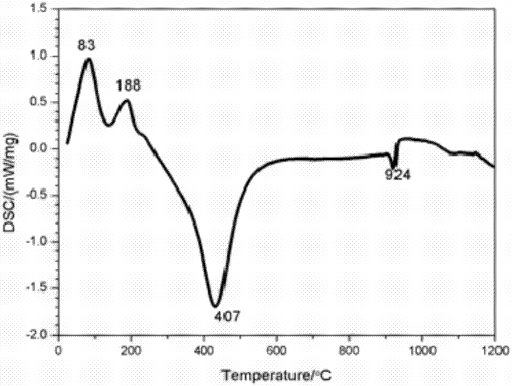
[0033] Grind 0.02mol of aluminum isopropoxide first, then add 50ml of ethylene glycol ether to ultrasonic for 10 minutes, stir at 70°C for 30 minutes; add 0.005mol of bismuth nitrate pentahydrate, and stir at 70°C for 30 minutes; add 0.02mol of ethyl orthosilicate, Stir at 70°C for 30 minutes; 0.02mol acetylacetone, continue to stir for 30 minutes; finally add 10ml of glacial acetic acid, stir at 90°C for 30 minutes, gradually cool to room temperature, and finally filter to obtain 60ml of sol precursor. The prepared colloid is thermally analyzed, and the data are as follows: figure 1 shown. The crystallization temperature of the sample is 924°C, indicating a high structural stability....
Embodiment 2
[0038] Fabrication of 210nm thick alumina-based film:
[0039] The steps of making alumina-based thin film are as follows:
[0040] A 210nm hydrated alumina dielectric film was prepared by spin coating on the surface of a Pt-plated silicon wafer, as follows:
[0041] Grind 0.04mol of aluminum isopropoxide first, then add 100ml of ethylene glycol ether to ultrasonic for 10min, stir at 70°C for 30 minutes; add 0.01mol of bismuth nitrate pentahydrate, stir at 70°C for 30 minutes; add 0.04mol of ethyl orthosilicate, Stir at 70°C for 30 minutes; 0.04mol acetylacetone, continue to stir for 30 minutes; finally add 20ml of glacial acetic acid, stir at 90°C for 30 minutes, gradually cool to room temperature, and finally filter to obtain 120ml of sol precursor.
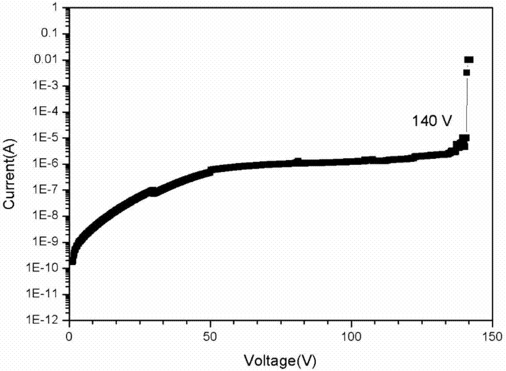
[0042] Thin films were obtained by spinning the colloid and heat-treated, and a layer of 120nm aluminum film was coated on the surface of the obtained films to test the breakdown field strength and leakage conductance. The st...
Embodiment 3
[0044] Fabrication of 270nm thick alumina-based film:
[0045] The steps of making alumina-based thin film are as follows:
[0046] A 270nm hydrated alumina dielectric film was prepared on the surface of a Pt-coated silicon wafer by spin coating. details as follows:
[0047] 1) the preparation of alumina base colloid is the same as embodiment 2
[0048] 2) Preparation of alumina-based film:
[0049] The film preparation steps are as follows:
[0050]Place the Pt-coated silicon wafer sample with a clean and dry surface on a homogenizer, then drop the sol precursor on the surface of the substrate, apply the sol evenly on the surface of the substrate at a speed of 3000 rpm, and then place the sample on the Dry heat treatment in the rapid heat treatment furnace. The pre-drying process conditions are 150°C for 2 minutes, 350°C for 2 minutes, and 450°C for 2 minutes. After reaching 9 layers, the prepared amorphous alumina with the required thickness is placed in the Heat treatm...
PUM
| Property | Measurement | Unit |
|---|---|---|
| Thickness | aaaaa | aaaaa |
| Thickness | aaaaa | aaaaa |
| Thickness | aaaaa | aaaaa |
Abstract
Description
Claims
Application Information