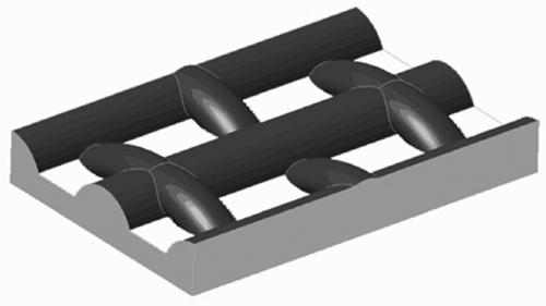
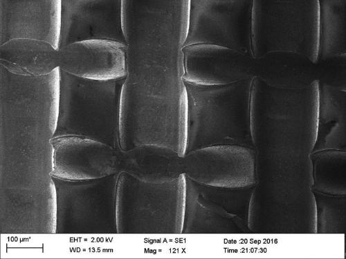
A preparation method of arched graphene three-dimensional network
A three-dimensional network and graphene technology, applied in the field of graphene, can solve the problems of slow and complicated transfer process, structural damage, collapse, etc., and achieve the effect of simplified process and simple process
- Summary
- Abstract
- Description
- Claims
- Application Information
AI Technical Summary
Problems solved by technology
Method used
Image
Examples
Embodiment 1
[0068] 1. Preparation of arched graphene three-dimensional network
[0069] Step 1: Take the three-dimensional copper mesh and cut it to 5 cm * 5 cm * 0.25 mm, take 100 mg of nickel wire with a diameter of 0.1 mm (120 mesh nickel powder can also be used in the specific practice process), and put the copper mesh and nickel wire into the 1:1 equal volume mixed alcohol and acetone mixed solution. Clean with ultrasonic waves at a power of 200-400W for 40-80 minutes, and then rinse repeatedly with deionized water to remove surface impurities and obtain a cleaned three-dimensional copper mesh.
[0070] Put the cleaned three-dimensional copper mesh and nickel wire (100 mg) into a vapor phase chemical deposition growth furnace. The volume of the furnace chamber is 1 liter, and the concentration of nickel vapor in the furnace chamber at the reaction temperature is about 0.13ppm (in the specific implementation process, Ensure that the concentration of nickel vapor in the reaction furna...
Embodiment 2
[0085] The basic experimental method of this embodiment is basically the same as that of Example 1. The difference is that in Step 1: the concentration of nickel vapor in the growth furnace cavity is about 0.05ppm at the reaction temperature of the experimental group, and no nickel wire is added to the control group.
[0086]The growth conditions of both the experimental group and the control group were as follows: the furnace temperature was 1010 degrees Celsius, the methane flow rate was 50 sccm, the hydrogen gas flow rate was controlled at 5 sccm, and the growth time was 60 minutes. All the other conditions and steps are the same as in Example 1.
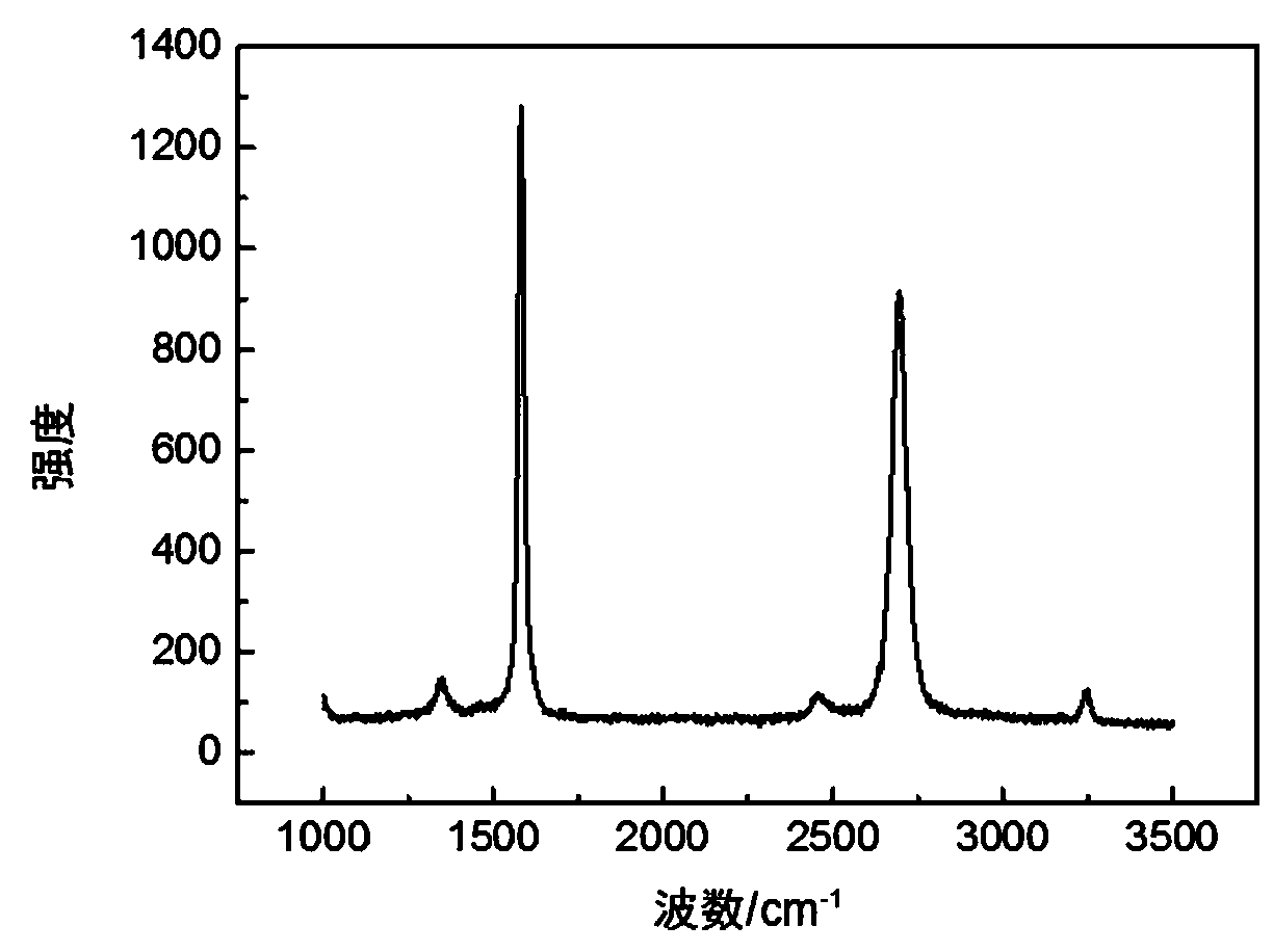
[0087] Figure 7 with Figure 8 They are the Raman spectra of the graphene networks of the experimental group (with nickel vapor added during growth) and the control group (without nickel vapor), respectively. From the Raman spectra, it can be seen that the graphene obtained in the experimental group is multi-layered, and the co...
Embodiment 3
[0091] The basic experimental method of this embodiment is basically the same as that of Example 1, except that in Step 1: the concentration of nickel vapor in the growth chamber of the experimental group in this embodiment is 2ppm at the reaction temperature, and the control group also does not add nickel.
[0092] The growth conditions of both the experimental group and the control group were: furnace temperature 990° C., methane flow rate 20 sccm, hydrogen flow rate control 15 sccm, and growth time 50 minutes. All the other conditions and steps are the same as in Example 1.
[0093] Figure 11 with Figure 12 Respectively, the Raman spectra of the experimental group (with nickel vapor added in the growth) and the control group (without nickel vapor) after the three-dimensional network transfer of the arched graphene. From the Raman spectrum, it can be seen that the graphene obtained by the experimental group is multi-layered. The control group was a single layer.
[0094...
PUM
| Property | Measurement | Unit |
|---|---|---|
| electrical resistance | aaaaa | aaaaa |
| electrical resistance | aaaaa | aaaaa |
| electrical resistance | aaaaa | aaaaa |
Abstract
Description
Claims
Application Information


