Metal-electroplating enhanced transparent conductive film and preparation method thereof
A technology of transparent conductive film and electroplating metal, which is applied in the direction of cable/conductor manufacturing, conductive layer on insulating carrier, circuit, etc., which can solve the problem that the structure cannot be well maintained, thermal stability is not ideal, and silver nanowires are damaged and other issues, to achieve good industrial application prospects, enhance light transmittance and electrical conductivity, and eliminate the effect of contact resistance
- Summary
- Abstract
- Description
- Claims
- Application Information
AI Technical Summary
Problems solved by technology
Method used
Image

Examples
Embodiment 1
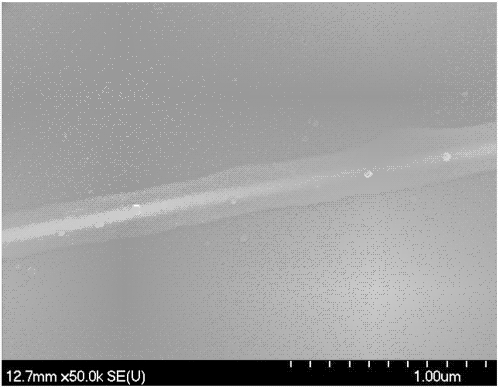
[0045] Select glass as the substrate, and use the spin coating method. First, spin-coating a layer of silane coupling agent KH-560 on the glass, and then spin-coating a layer of silver nanowires on the glass to obtain a transparent conductive layer with visible light transmittance It is about 98.6%, the sheet resistance is about 600Ω / sq, and the rotation speed used in the spin coating process is 2000r / min.
[0046] Then, electroplating is used to plate the samples obtained above with nickel. The specific formulation of the electroplating solution used in this embodiment is: 100g / L nickel sulfate, 18g / L nickel chloride, 11g / L boric acid, 1ml / L main light agent HN-8, 1ml / L wetting agent HN-19, adjust The pH is about 3.5. During the electroplating process, the current density used is about 3mA / cm 2 , The plating time is 5min.
[0047] After electroplating, the sample is washed with deionized water and ethanol, and dried naturally to obtain a transparent conductive film product. figu...
Embodiment 2
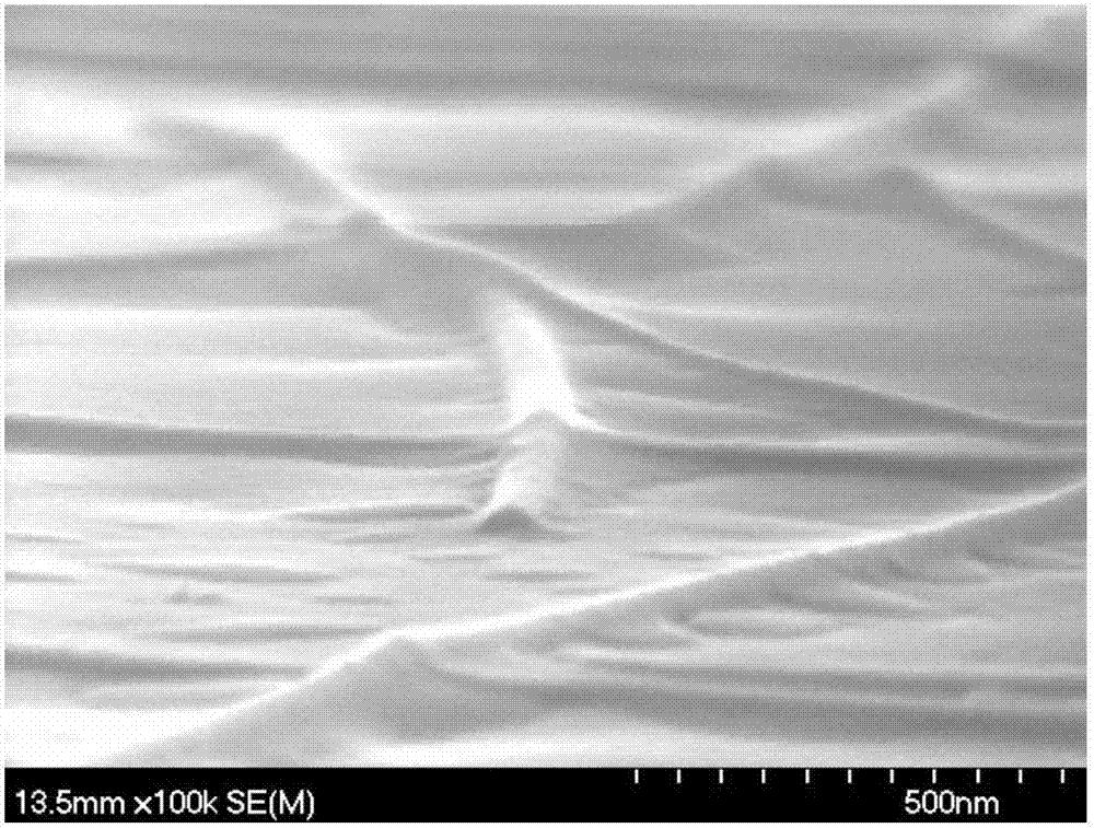
[0049] Select glass as the substrate, and use the spin coating method. First, spin-coating a layer of silane coupling agent KH-560 on the glass, and then spin-coating a layer of silver nanowires on the glass to obtain a transparent conductive layer with visible light transmittance It is about 98.6%, and the sheet resistance is about 600Ω / sq. The speed used in the spin coating process is 2000r / min.
[0050] Then, electroplating is used to plate the samples obtained above with nickel. The specific formulation of the electroplating solution used in this embodiment is: 50g / L nickel sulfate, 9g / L nickel chloride, 6g / L boric acid, 1ml / L main light agent HN-8, 1ml / L wetting agent HN-19, adjust The pH is about 3.5. During the electroplating process, the current density used is about 8mA / cm 2 , The plating time is 15s.
[0051] The sample obtained after electroplating is washed with deionized water and ethanol to finally obtain a transparent conductive film product. figure 2 A scanning ...
Embodiment 3
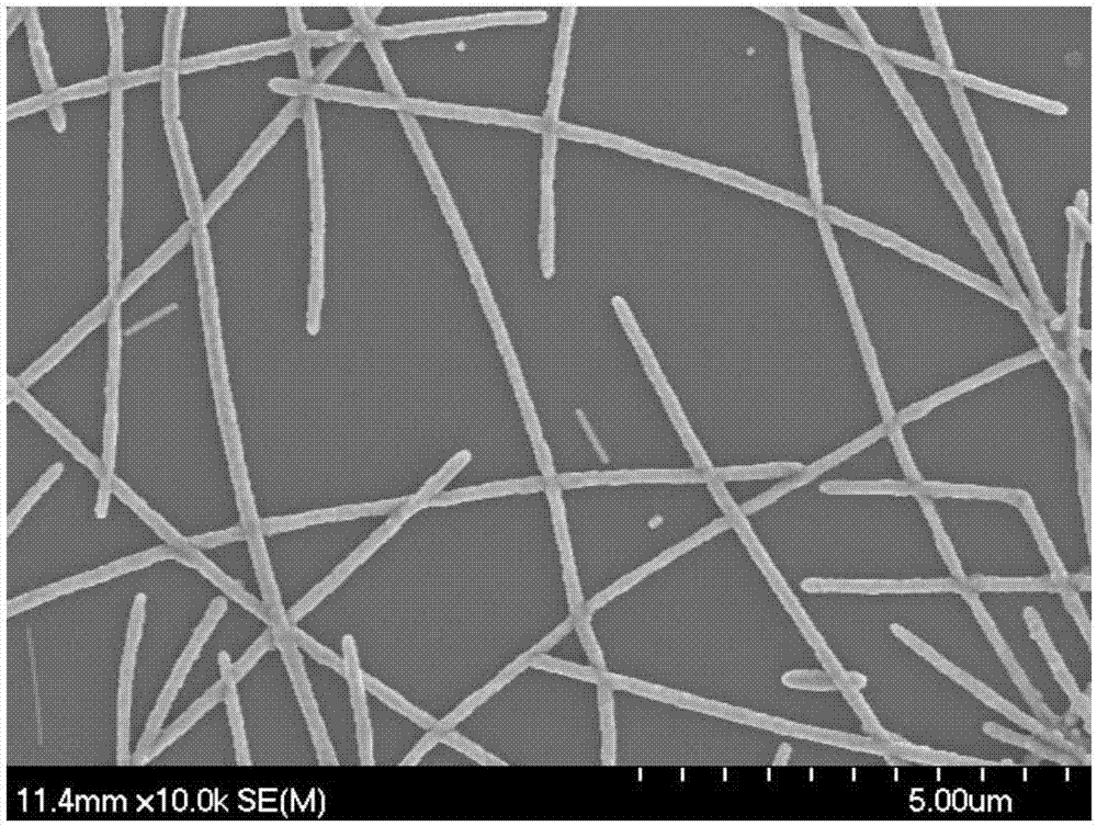
[0053] PET is selected as the substrate, and a layer of silver nanowires is directly pulled on the PET by the pulling method to obtain a transparent conductive layer with a visible light transmittance of about 99.0% and a sheet resistance of about 1200Ω / sq.
[0054] Then electroplating is used to plate the samples obtained above with copper. The specific formulation of the electroplating solution used in this embodiment is: 200 g / L copper sulfate, 70 g / L sulfuric acid, 0.06 g / L hydrochloric acid, 0.1 g / L sodium lauryl sulfate, and 0.0001 g / L tetrahydrothiazolthione. During the electroplating process, the current density used is about 10mA / cm 2 , The plating time is 10s.
[0055] The sample obtained after electroplating is washed with deionized water and ethanol, and finally freeze-dried in vacuum to obtain a transparent conductive film product. image 3 A scanning electron microscope picture of the prepared transparent conductive film is given. It can be seen that the silver nanowi...
PUM
| Property | Measurement | Unit |
|---|---|---|
| thickness | aaaaa | aaaaa |
| thickness | aaaaa | aaaaa |
| diameter | aaaaa | aaaaa |
Abstract
Description
Claims
Application Information
 - R&D
- Intellectual Property
- Life Sciences
- Materials
- Tech Scout
- Unparalleled Data Quality
- Higher Quality Content
- 60% Fewer Hallucinations
Browse by: Latest US Patents, China's latest patents, Technical Efficacy Thesaurus, Application Domain, Technology Topic, Popular Technical Reports.
© 2025 PatSnap. All rights reserved.Legal|Privacy policy|Modern Slavery Act Transparency Statement|Sitemap|About US| Contact US: help@patsnap.com