Zinc oxide transparent electrode-based opposed-contact photoconductive switch and fabrication method thereof

A technology of photoconductive switch and transparent electrode, which is applied in the field of microelectronics, can solve the problems of inability to achieve low energy density triggering, limited laser incident area, and increase the difficulty of devices, so as to achieve flexible and convenient design, reduce design difficulty, and increase laser concentration. Effect

Active Publication Date: 2017-06-30
XIDIAN UNIV
View PDF4 Cites 1 Cited by
  • Summary
  • Abstract
  • Description
  • Claims
  • Application Information

AI Technical Summary

Problems solved by technology

[0005] On the one hand, the 532nm laser needs to be irradiated from two sides, and the laser incident area on the side of the device is extremely limited. In this case, the use of the device requires a sophisticated optical fiber system to build an optical path for the switch, which increases the difficulty of using the device.
[0006] On the other hand, when the 532nm laser is irradiated from the side and reaches the bottom of the electrode, the energy of the laser has been greatly attenuated. To reach the saturation state of the device, the energy density of the incident laser needs to be increased, that is, in principle, low energy density triggering cannot be achieved.

Method used


Image

  • Zinc oxide transparent electrode-based opposed-contact photoconductive switch and fabrication method thereof
  • Zinc oxide transparent electrode-based opposed-contact photoconductive switch and fabrication method thereof
  • Zinc oxide transparent electrode-based opposed-contact photoconductive switch and fabrication method thereof

Examples


Embodiment 1

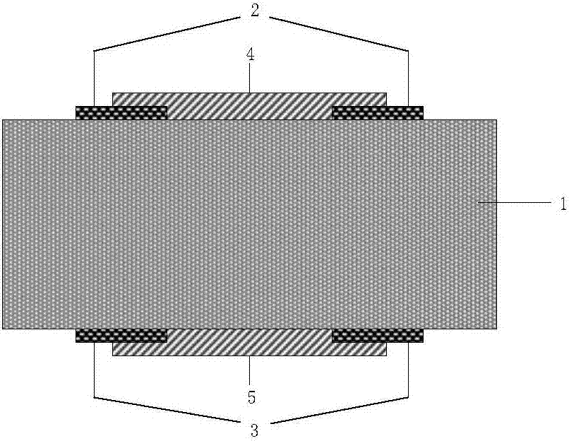
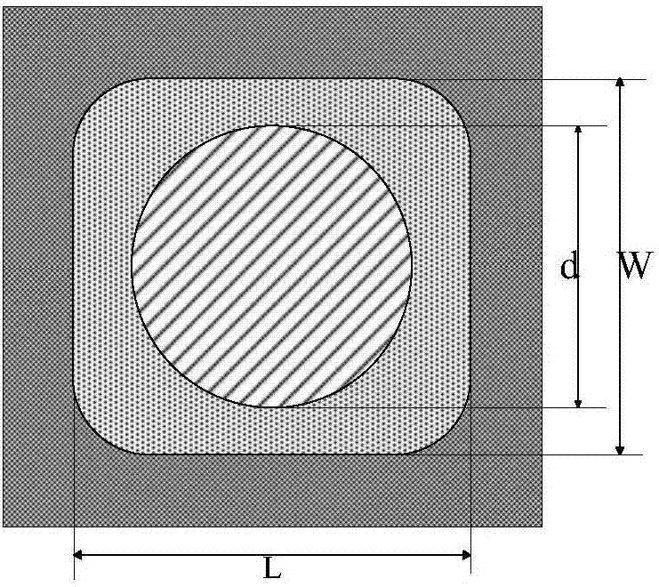
[0033] Example 1, making a transparent electrode different-surface photoconductive switch. The diameter d of the bottom surface of the upper film electrode and the lower film electrode is 6mm, and the thickness is 1μm.

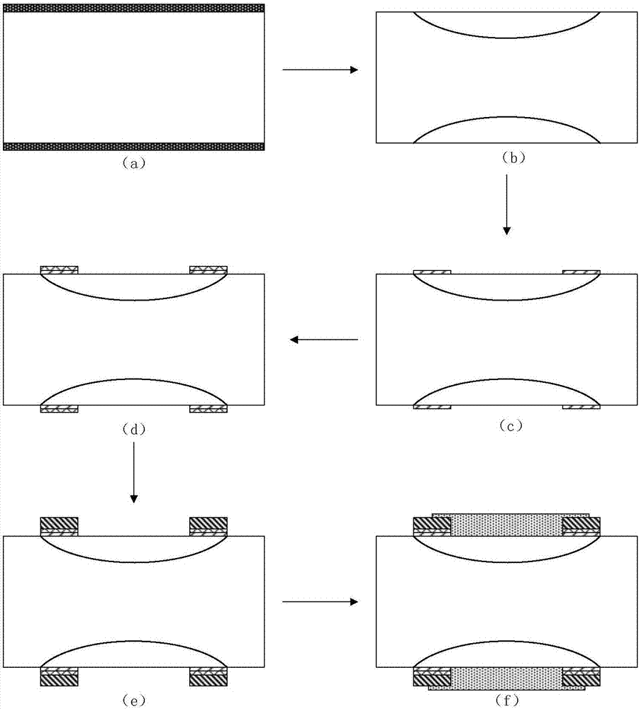
[0034] Step 1: Deposit barrier layers on the front and back of the vanadium-doped silicon carbide substrate sample respectively.

[0035] Using the PECVD method to deposit silicon dioxide with a thickness of 2 μm on the front and back of the rectangular parallelepiped silicon carbide substrate sample, as a barrier layer for ion implantation on the front and back of the substrate; image 3 a.

[0036] Step 2: Perform ion implantation on the front and back of the sample respectively.

[0037] (2a) Apply glue on the barrier layer on the front and back of the sample respectively, etch the ion implantation window on the barrier layer after coating with a photolithography plate, and use HF acid with a concentration of 5% to etch away the barrier layer under the wi...

Embodiment 2

[0053] Example 2, making a transparent electrode different-surface photoconductive switch. The diameter d of the bottom surface of the upper film electrode and the lower film electrode is 6.5mm, and the thickness is 1.5μm. The thickness of the upper ohmic contact electrode and the lower ohmic contact electrode is 1.165μm.

[0054] Step 1: Deposit barrier layers on the front and back of the vanadium-doped silicon carbide substrate sample respectively.

[0055] Using the PECVD method to deposit silicon dioxide with a thickness of 2.5 μm on the front and back of the rectangular parallelepiped silicon carbide substrate sample, as a barrier layer for ion implantation on the front and back of the substrate; image 3 a.

[0056] Step 2: Perform ion implantation on the front and back of the sample respectively.

[0057] First, apply glue on the barrier layer on the front and back of the sample respectively, use a photolithography plate to etch the ion implantation window on the barr...

Embodiment 3

[0073] Example 3, making a transparent electrode different-surface photoconductive switch. The diameter d of the bottom surface of the upper film electrode and the lower film electrode is 7mm, and the thickness is 2μm.

[0074] Step A: Depositing the front and back of the vanadium-doped silicon carbide substrate respectively.

[0075] Using the PECVD method to deposit silicon dioxide with a thickness of 3 μm on the front and back of the rectangular parallelepiped silicon carbide substrate sample, as a barrier layer for ion implantation on the front and back of the substrate; image 3 a

[0076] Step B: performing ion implantation on the front and back of the sample respectively.

[0077] (Ba) Apply glue on the barrier layer on the front and back of the sample respectively, etch the ion implantation window on the barrier layer after coating with a photolithography plate, and etch the barrier layer under the window position with HF acid with a concentration of 5%. , and remov...


PUM

PropertyMeasurementUnit
widthaaaaaaaaaa
thicknessaaaaaaaaaa
diameteraaaaaaaaaa

Abstract

The present invention discloses a zinc oxide transparent electrode-based opposed-contact photoconductive switch. The zinc oxide transparent electrode-based opposed-contact photoconductive switch includes a vanadium-doped silicon carbide substrate (1), an upper ohmic contact electrode (2), a lower ohmic contact electrode (3), an upper thin film electrode (4) and a lower thin film electrode (5); the upper ohmic contact electrode (2) and the lower ohmic contact electrode (3) are respectively deposited on the front surface and back surface of the vanadium-doped silicon carbide substrate (1); the upper thin film electrode (4) is deposited on the front surface of the vanadium-doped silicon carbide substrate (1) and the surface of the upper ohmic contact (2); the lower thin film electrode (5) is deposited on the back surface of the vanadium-doped silicon carbide substrate (1) and the surface of the lower ohmic contact electrode (3); the upper thin film electrode and the lower thin film electrode are both made of a transparent zinc oxide material; and therefore, the photoconductive switch can be turned on when the surfaces of the electrodes are under illumination, and the light receiving area of the device is increased, the photon concentration and laser energy utilization rate of a conductive channel can be improved. The photoconductive switch can be used for a high-speed pulse system.

Description

technical field [0001] The invention belongs to the field of microelectronics, in particular to a transparent electrode different-surface photoconductive switch, which can be used as a switch in a high-speed and high-power pulse system. [0002] technical background [0003] In 1974, D.H.Auston of Bell Laboratories prepared the world's first silicon-based photoconductive switch, but due to the limitations of silicon materials, high-performance switches could not be obtained; in 1976, H.L.Chi of the University of Maryland prepared the first The first GaAs photoconductive switch, its performance is far superior to the silicon-based photoconductive switch, so in the following decades, the photoconductive switch of gallium arsenide has been relatively mature research. However, due to the unique Lock-on effect of the GaAs photoconductive switch, its application in a wider range is limited. With the maturity of the third-generation semiconductor silicon carbide material, it has gr...

Claims


Application Information

Patent Timeline
Patent Type & Authority Applications(China)
IPC IPC(8): H01L31/08H01L31/0224H01L31/18
CPCH01L31/0224H01L31/022408H01L31/08H01L31/18Y02P70/50
Inventor 郭辉吴建鲁曹鹏辉张玉明张晨旭
Owner XIDIAN UNIV
Why Eureka
Try Eureka