Preparation method for growing ABX3-type perovskite thin film through single-step in-situ flash method

A technology of perovskite and flash evaporation is applied in the preparation of perovskite thin films. The field of perovskite thin films prepared by deposition process can solve the problem that the rate is not suitable for large-scale production, cannot be mass-produced, and single-crystal silicon is time-consuming. Energy consumption and other issues, to achieve the effect of a wide selection of substrates, good crystal quality of the film, and easy operation

Inactive Publication Date: 2017-07-04
SHANGHAI UNIV
View PDF3 Cites 16 Cited by
  • Summary
  • Abstract
  • Description
  • Claims
  • Application Information

AI Technical Summary

Problems solved by technology

But monocrystalline silicon consumes time and energy
Although the second-generation solar cells save materials and have low growth costs, they also have unavoidable shortcomings. Te, In, Ga, etc. are elements with little reserves on the earth, and they are more scarce than Au, which will make them unable to be mass-produced , greatly affecting its output value
However, the control of the dual-source metho

Method used


Image

  • Preparation method for growing ABX3-type perovskite thin film through single-step in-situ flash method
  • Preparation method for growing ABX3-type perovskite thin film through single-step in-situ flash method
  • Preparation method for growing ABX3-type perovskite thin film through single-step in-situ flash method

Examples


Embodiment 1

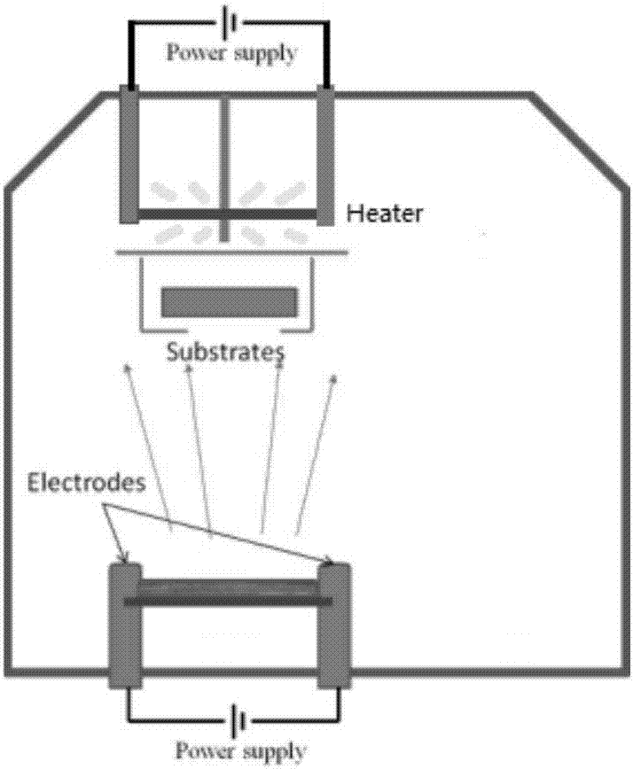
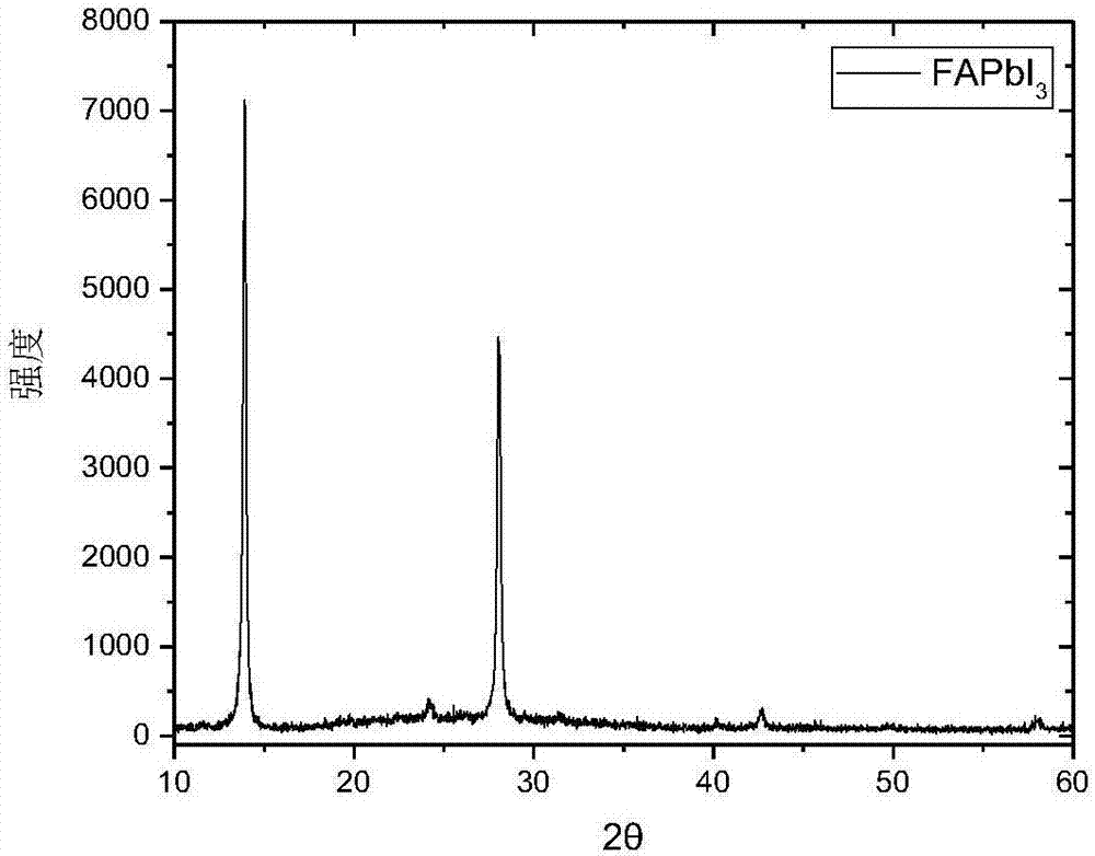
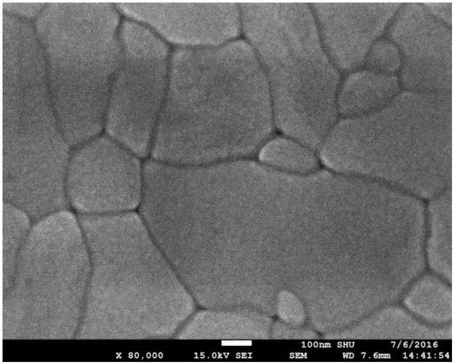
[0026] In this example, see figure 1 , a single-step in situ flash method for growing FAPbI 3 The preparation method of perovskite thin film, comprises the steps:

[0027] a. Substrate pretreatment:

[0028] F-doped SnO 2 FTO, the transparent conductive glass SnO 2 : F as a deposition substrate, the pretreatment steps are:

[0029] First use zinc powder and dilute hydrochloric acid to etch the FTO transparent conductive glass substrate to form the required pattern, then rinse it with deionized water, and then use Triton to clean the substrate surface to remove the stains on the substrate surface, and then use deionized water to clean the surface of the substrate. Wash with water, rinse off the residual triton on the surface of the substrate, then use acetone and ethanol to ultrasonically clean for 15 minutes, then rinse the surface of the FTO transparent conductive glass substrate with deionized water, and then dry the FTO transparent conductive glass substrate , and fina...

Embodiment 2

[0037] This embodiment is basically the same as Embodiment 1, especially in that:

[0038] In this example, a single-step in situ flash method for growing FAPbI 3 The preparation method of perovskite thin film, comprises the steps:

[0039] a. Substrate pretreatment:

[0040] The Si substrate is adopted, and the Si substrate is used as a deposition substrate. The pretreatment steps are:

[0041] The Si substrate is cleaned with deionized water, and then the Si substrate is soaked in concentrated sulfuric acid with a concentration of 98.3% by mass percentage, then the Si substrate is taken out, and the residual sulfuric acid on the Si substrate is cleaned with deionized water, and then the Si substrate is treated. Drying is carried out, and finally the surface of the Si substrate is treated with microwave plasma for 10 minutes to obtain a clean silicon substrate;

[0042] Then take 5mg PCBM and dissolve it in 1ml of chlorobenzene, stir at room temperature for 12h, make it fu...


PUM


Abstract

The invention discloses a preparation method for growing an ABX3-type perovskite thin film through a single-step in-situ flash method. The preparation method is applied to the field of manufacturing processes for novel materials. The preparation method for the perovskite thin film comprises the following steps: taking the solution of a perovskite material as a single evaporation source; adding a heating device to a substrate; rapidly increasing a current to be not lower than 200A instantaneously under the condition that the temperature of the substrate of a sample is certain after a vacuum degree achieves a certain requirement, so that the temperature of an evaporation boat achieves a temperature of not lower than 1000 DEG C instantaneously, and the material is sublimated instantaneously; and finally directly carrying out post-annealing on the material in a vacuum cavity body to obtain the stable ABX3-type perovskite thin film. The perovskite thin film prepared by the preparation method disclosed by the invention through the single-step in-situ flash method is low in energy consumption, high in evaporation speed, short in time, void-free and uniform in large area, wide in substrate selection range, and suitable for a planar device.

Description

technical field [0001] The invention relates to a method for preparing a perovskite thin film, in particular to a method for preparing a perovskite thin film through a deposition process, which is applied in the technical field of photoelectric device preparation. Background technique [0002] In today's society, human beings are developing rapidly, and the development of human society is inseparable from energy. For a long time, the main energy sources used by human beings are non-renewable energy sources such as coal, oil and natural gas. Since the beginning of the 21st century, with the rapid improvement of people's production and life, the demand and consumption of energy have also increased significantly, and non-renewable energy is facing a crisis of depletion. Therefore, it is urgent to find new and clean renewable energy. At present, a variety of new energy sources are constantly being utilized and developed, such as solar energy, water energy, and wind energy. Amo...

Claims


Application Information

Patent Timeline
IPC IPC(8): C23C14/12C23C14/02C23C14/24C23C14/58H01L51/00
CPCC23C14/021C23C14/12C23C14/243C23C14/5806H10K71/164
Inventor 崔四维倪超伟刘风采焦钰清蔡江张新月徐闰
Owner SHANGHAI UNIV
Why Eureka
Try Eureka