Perovskite solar cell and preparation method thereof
A solar cell and perovskite technology, applied in the field of solar cells, can solve the problems of easily affecting the electrical properties of solar cell device resistance, open circuit voltage fill factor, surface plasmon effect enhancement effect, randomness and uncontrollability, etc. , to achieve high production and application value, improve photoelectric conversion efficiency, and high flexibility
- Summary
- Abstract
- Description
- Claims
- Application Information
AI Technical Summary
Problems solved by technology
Method used
Image

Examples
preparation example Construction
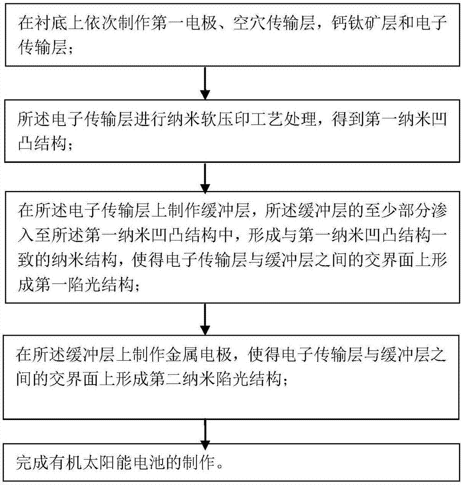
[0062] (9) Complete the preparation of the perovskite solar cell.
[0063] In order to effectively improve the photoelectric conversion efficiency of the perovskite solar cell in the embodiment of the present invention, a nano light-trapping structure is set on the buffer layer corresponding to the electron transport layer of the perovskite solar cell and its upper layer, and the metal electrode, and the nanostructure increases by scattering. The length of the optical path and the realization of the surface plasmon effect can effectively increase the light absorption of the photoactive layer, thereby effectively improving the photoelectric conversion efficiency of the present invention.
[0064] In the preparation process of the present invention, the soft nano-imprinting process is used to prepare the nano-concave-convex structure, which effectively ensures the high fidelity of the copying and transferring process, and at the same time realizes one-step imprinting forming, whe...
Embodiment 1
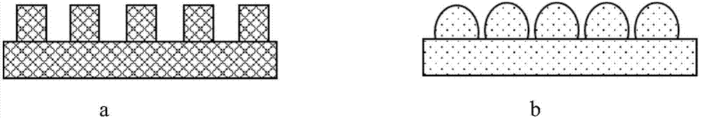
[0070] Such as figure 2 As shown in (a), in one embodiment, the shape of the nano concave-convex structure used is a one-dimensional periodic grating structure with a groove depth of 80 nm and a period of 500 nm.
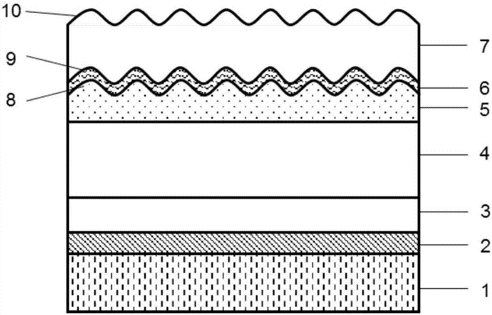
[0071] The specific manufacturing process of each layer structure of the transparent electrode 2, the hole transport layer 3, the perovskite light absorption layer 4, the electron transport layer 5, the buffer layer 6 and the metal electrode 7 on the substrate 1 can be respectively selected from the solution method. Coating, vapor deposition, sputtering and other methods, or other known methods, preferably, such as image 3 As shown, in this embodiment, the specific process is as follows:
[0072](1) On the other surface of common float glass (as substrate 1) sputtering generates ITO thin film, carries out photolithographic treatment to ITO thin film, cuts into required size, and this ITO thin film is as first electrode 2, then, to The ITO film was ultrasonically...
Embodiment 2
[0086] Such as figure 2 As shown in (b), the nano-concave-convex structure is a two-dimensional quasi-periodic moth-eye shape, the groove depth is 80nm, and the period is 400nm. Of course, in other embodiments, the relevant specific parameters of the nano-concave-convex structure can be selected according to actual needs. , so as to obtain the first nanometer light-trapping structure with different periods, which is not specifically limited in the present invention.
[0087] The specific manufacturing process of each layer structure of the first electrode 2, the hole transport layer 3, the perovskite layer 4, the electron transport layer 5, the buffer layer 6 and the metal electrode 6 on the substrate 1 can be selected from solution method spin coating, Methods such as vapor deposition, sputtering, or other known methods, preferably, such as image 3 As shown, in the embodiment, the specific process is as follows:
[0088] (1) On the other surface of common float glass (as ...
PUM
| Property | Measurement | Unit |
|---|---|---|
| Thickness | aaaaa | aaaaa |
Abstract
Description
Claims
Application Information
 - Generate Ideas
- Intellectual Property
- Life Sciences
- Materials
- Tech Scout
- Unparalleled Data Quality
- Higher Quality Content
- 60% Fewer Hallucinations
Browse by: Latest US Patents, China's latest patents, Technical Efficacy Thesaurus, Application Domain, Technology Topic, Popular Technical Reports.
© 2025 PatSnap. All rights reserved.Legal|Privacy policy|Modern Slavery Act Transparency Statement|Sitemap|About US| Contact US: help@patsnap.com