Tantalum sputtering target, and production method therefor

The technology of sputtering target and diffraction method is applied in the field of tantalum sputtering target, which can solve the problems of high film formation speed and uncontrollable film thickness uniformity, and achieve the effect of excellent film thickness uniformity.

Active Publication Date: 2017-08-29
JX NIPPON MINING & METALS CORP
View PDF19 Cites 1 Cited by
  • Summary
  • Abstract
  • Description
  • Claims
  • Application Information

AI Technical Summary

Problems solved by technology

On the other hand, the wiring width of semiconductor integrated circuits is being miniaturized. In high-power sputtering, there is a problem that in order to form a uniform film on the state-of-the-art fine wiring pattern, the film formation speed is too high and cannot Control the uniformity of film thickness
In particular, this problem is significant when an extremely thin film is formed in a wiring hole with a large aspect ratio.

Method used


Image

  • Tantalum sputtering target, and production method therefor
  • Tantalum sputtering target, and production method therefor
  • Tantalum sputtering target, and production method therefor

Examples


Embodiment 1

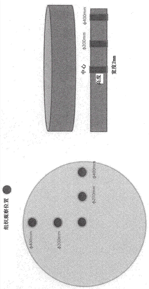
[0046] A tantalum raw material with a purity of 99.997% was electron beam melted and cast to produce an ingot with a length of 1000 mm and a diameter of 195 mmφ. Next, this ingot was subjected to cold press forging to have a diameter of 150 mm, and then cut to a required length to obtain a billet. Next, heat treatment was performed at a temperature of 1250°C, cold forging was performed once again, heat treatment was performed at 1000°C, followed by secondary cold forging, divided into 2 parts, and heat treatment was performed again at 1000°C.

[0047] Next, cold rolling is performed on the forged billet. For the rolling process, the continuous rolling passes with a reduction ratio of less than 6% were repeated 30 times in total, and then rolling was performed in the rolling passes with a reduction ratio of 6% or more. After rolling, it is heat treated at 800°C. Next, a tantalum sputtering target with a thickness of 6.35 mm and 450 mmφ was produced by machining the obtained t...

Embodiment 2-5

[0050] A forged billet was produced by the same method as in Example 1 or the like. Next, cold rolling is performed on the forged billet. In the rolling process, as shown in Table 1, the total number of continuous rolling passes with a reduction ratio of less than 6% is adjusted, and then rolling is carried out with a rolling pass with a reduction ratio of 6% or more, so that the total reduction ratio Reach more than 85%. After rolling, heat treatment is performed at 800°C. Next, a tantalum sputtering target with a thickness of 6.35 mm and 450 mmφ was produced by machining the obtained target material with a thickness of 10 mm and 500 mmφ.

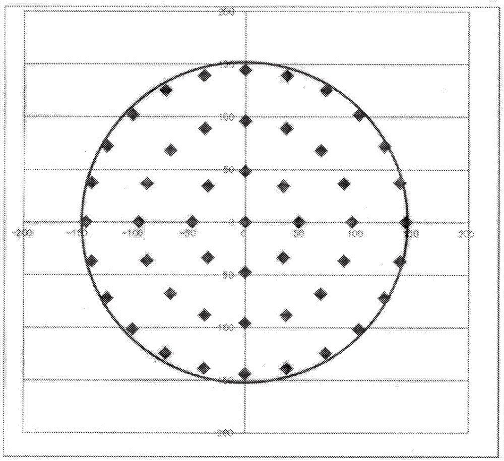
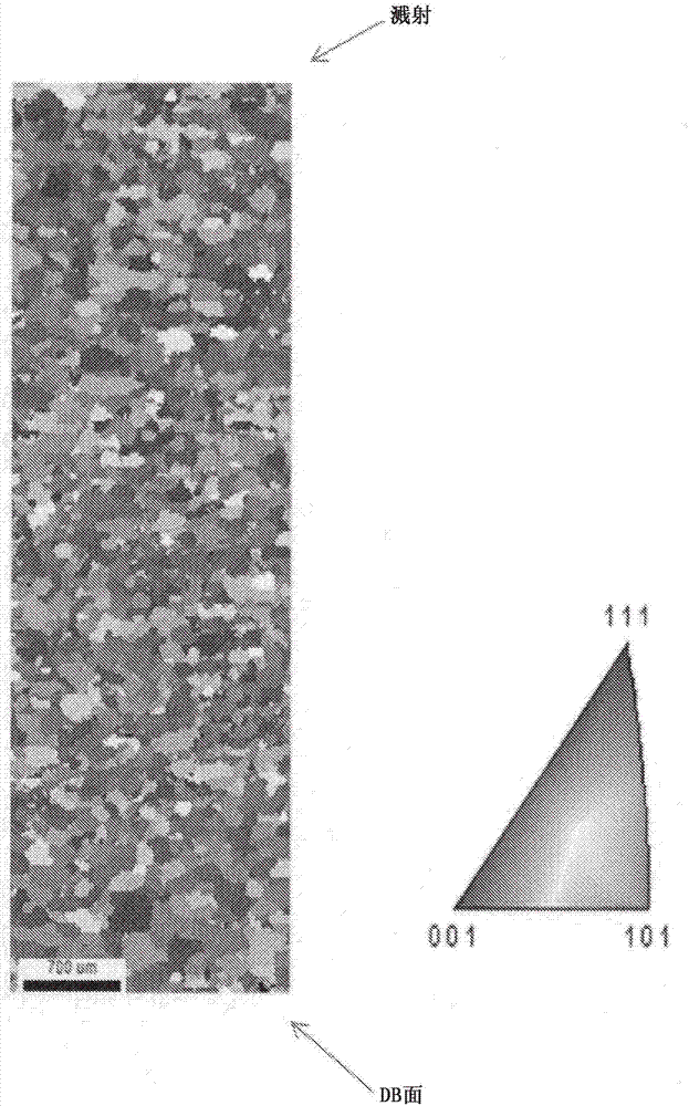
[0051] About the sputtering target obtained by the above process, the structure of the cross section perpendicular|vertical to the sputtering surface of a target was observed using the method similar to Example 1. As a result, the area ratios of crystal grains in which the {100} planes were oriented along the ND were all 30% or more. M...


PUM


Abstract

When backscattered electron diffraction is used to observe the normal direction ND of the rolling surface, i.e. a cross section orthogonal to the sputtering surface of the target, this tantalum sputtering target has an area ratio of crystal grains of which the {100} plane is oriented in ND of at least 30%. The present invention addresses the problem of providing a tantalum sputtering target with which the film-formation rate can be suitably controlled under high-power sputtering conditions. When such a tantalum target is used to form a film by way of sputtering, a thin film exhibiting excellent film-thickness uniformity can be formed, and productivity of the thin film formation process can be improved, even with regard to fine wiring.

Description

technical field [0001] The present invention relates to a tantalum sputtering target suitable for the formation of a barrier seed layer in the wiring of a semiconductor integrated circuit, and in particular to a sputtering rate (film formation speed) that can be achieved even under high-power sputtering by moderately reducing the sputtering rate. Tantalum sputtering target with good film thickness uniformity and manufacturing method thereof. Background technique [0002] The sputtering method for forming a coating of metal or ceramic material is used in many fields such as electronics, corrosion-resistant materials or decoration, catalysts, cutting / abrasive materials, and wear-resistant materials. The sputtering method itself is a well-known method in the above-mentioned field, but recently, especially in the field of electronics, a tantalum sputtering target suitable for forming a complex-shaped film or forming a circuit has been demanded. [0003] Generally speaking, the ...

Claims


Application Information

Patent Timeline
Patent Type & Authority Applications(China)
IPC IPC(8): C23C14/34C22C27/02C22F1/00C22F1/18
CPCC23C14/34C22C27/02C22F1/00C22F1/18B22D7/005H01J37/3426C23C14/3414C23C14/14
Inventor 永津光太郎仙田真一郎
Owner JX NIPPON MINING & METALS CORP
Why Eureka
Try Eureka