Avalanche photo-diode based on AlInAsSb body material as multiplication region and preparation method therefor

An avalanche photoelectric and diode technology, applied in circuits, electrical components, semiconductor devices, etc., can solve problems such as low detection sensitivity, thermal noise limitation of detection sensitivity, and increase system operating costs, achieving high gain-bandwidth product and meeting sensitivity requirements , Reduce the effect of tunneling dark current

Inactive Publication Date: 2017-09-15
INST OF SEMICONDUCTORS - CHINESE ACAD OF SCI
View PDF8 Cites 16 Cited by
  • Summary
  • Abstract
  • Description
  • Claims
  • Application Information

AI Technical Summary

Problems solved by technology

[0003] Among the existing photodetectors, the PIN photodiode has the advantages of simple structure, easy manufacturing process, high reverse bias voltage, and wide linear output range. Its typical device silicon PIN large-area photodetector is widely used in laser detection system, fast pulse detector, etc., but because the intrinsic I-layer resistance of the PIN photodiode is large and the output current is small, its detection sensitivity is relatively low when detecting weak light, and it is necessary to pre-amplify the signal. This makes the detection sensitivity limited by the thermal noise of the external amplifier, shortens the relay distance of the communication system, increases the number of relay stations required, and increases the operating cost of the entire system; and the avalanche photodiode (Avalanche Photo- diode, APD) can provide 5dB~10dB higher sensitivity than PIN phot

Method used


Image

  • Avalanche photo-diode based on AlInAsSb body material as multiplication region and preparation method therefor
  • Avalanche photo-diode based on AlInAsSb body material as multiplication region and preparation method therefor
  • Avalanche photo-diode based on AlInAsSb body material as multiplication region and preparation method therefor

Examples


Example Embodiment

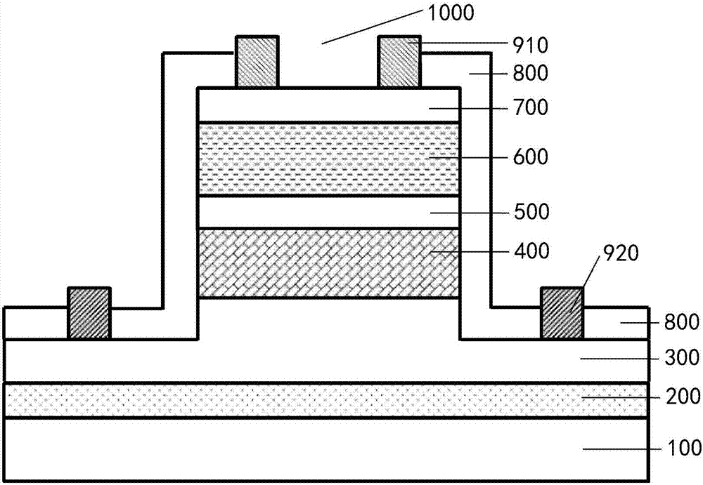
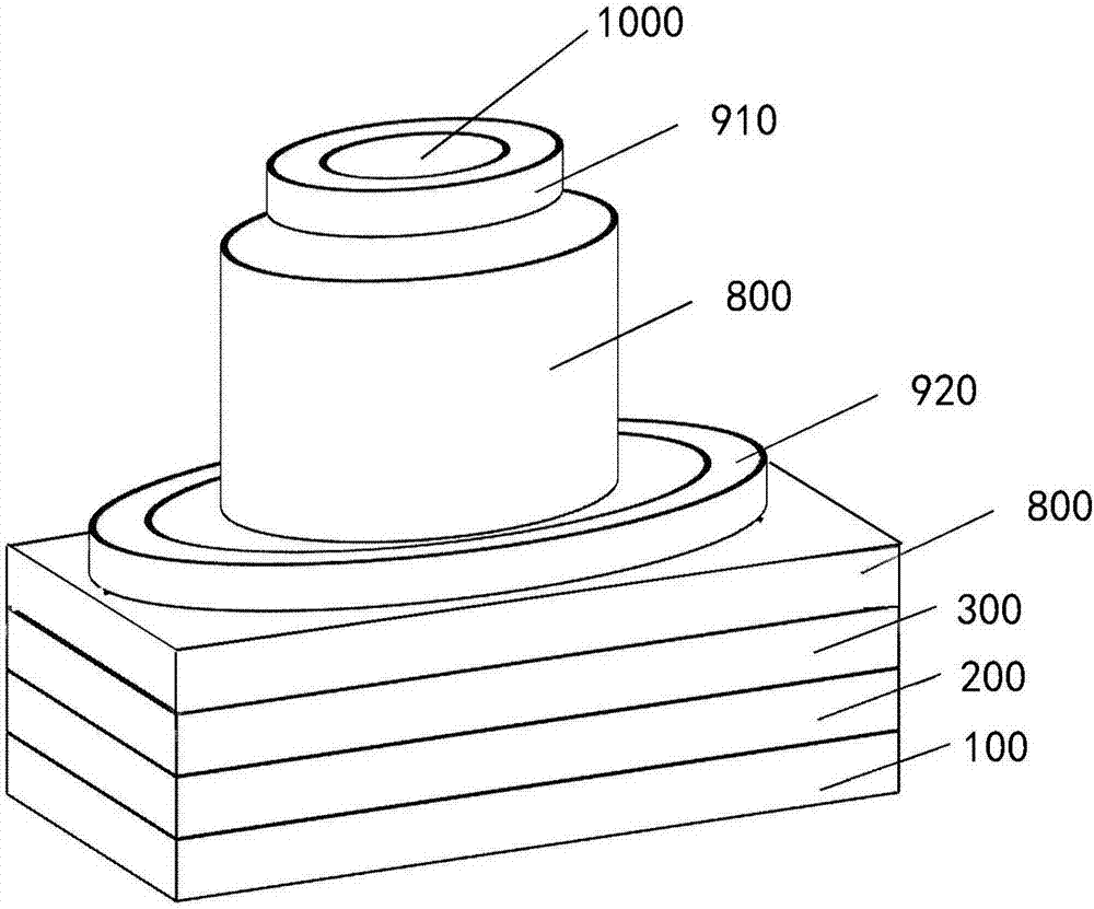
[0039] The invention provides an avalanche photodiode based on the AlInAsSb bulk material as the multiplication zone and a preparation method thereof. By using the AlInAsSb bulk material as the avalanche multiplying layer, it has the characteristics of single-carrier ionization, and there is no avalanche build-up time. The gain-bandwidth product limit has the advantages of low noise and high gain-bandwidth product. At the same time, the forbidden band width can be adjusted by using substrates with different lattice constants, which effectively reduces the dark current and satisfies the requirements of photodetectors. While requiring high sensitivity, the design of energy band engineering can also be realized, which broadens its scope of application.
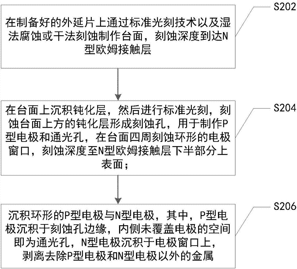
[0040] In order to make the objectives, technical solutions, and advantages of the present invention clearer, the present invention will be further described in detail below in conjunction with specific embodiments and with reference...


PUM

PropertyMeasurementUnit
Thicknessaaaaaaaaaa
Thicknessaaaaaaaaaa
Thicknessaaaaaaaaaa

Abstract

The invention provides an avalanche photodiode based on AlInAsSb body material as the multiplication region, comprising: a substrate; a buffer layer epitaxially on the substrate; an N-type ohmic contact layer epitaxially on the buffer layer and having a cross section of "" Convex" shape, its lower half is consistent with the shape of the substrate, and its upper half is cylindrical; the avalanche multiplication layer is epitaxial on the upper surface of the upper half of the N-type ohmic contact layer, composed of AlxIn1‑xAsySb1‑y Bulk material preparation, the doping concentration is less than 1016cm-3, the value range of x is: 0≤x≤1, the value range of y is: 0.08≤y≤1; the P-type charge layer is epitaxial on the avalanche multiplication layer ; The light absorbing layer is epitaxial on the P-type charge layer; and the P-type ohmic contact layer is epitaxially on the light absorbing layer. The avalanche photodiode has the advantages of low noise and high gain-bandwidth product, and at the same time effectively reduces the dark current, which not only meets the requirement of high sensitivity of the photodetector, but also realizes the design of energy band engineering and broadens its application range.

Description

technical field [0001] The invention belongs to the field of semiconductor devices, in particular to an avalanche photodiode based on an AlInAsSb bulk material as a multiplication region and a preparation method thereof. Background technique [0002] Photoelectric detectors have a wide range of uses in various fields of military and national economy. They are mainly used for ray measurement and detection, industrial automatic control, photometry, etc. in the visible or near-infrared band; they are mainly used in missile guidance and infrared thermal imaging in the infrared band. , infrared remote sensing, etc. In recent years, due to the rapid development of optical communication systems, the requirements for receiver responsivity and response speed are getting higher and higher, and higher requirements are also put forward for the sensitivity of photodetectors. [0003] Among the existing photodetectors, the PIN photodiode has the advantages of simple structure, easy manuf...

Claims


Application Information

Patent Timeline
IPC IPC(8): H01L31/0304H01L31/107H01L31/18
CPCH01L31/1075H01L31/03042H01L31/03046H01L31/1844
Inventor 吕粤希孙姚耀郭春妍王国伟徐应强牛智川
Owner INST OF SEMICONDUCTORS - CHINESE ACAD OF SCI
Why Eureka
Try Eureka