Preparation method of composite structured GaN/CdZnTe thin film ultraviolet light detector

A composite structure and detector technology, used in semiconductor/solid-state device manufacturing, semiconductor device, final product manufacturing, etc., can solve problems such as the inability to guarantee the normal use of ultraviolet light detectors, and achieve good stability, light response, and high thermal conductivity. , The effect of high chemical inertness

Active Publication Date: 2017-09-15
SHANGHAI UNIV
View PDF3 Cites 3 Cited by
  • Summary
  • Abstract
  • Description
  • Claims
  • Application Information

AI Technical Summary

Problems solved by technology

However, traditional Si, GaAs and other materials are used as substrates, and the normal use of ultraviolet light detectors under high temperature and strong radiation conditions cannot be guaranteed due to the too small bandgap.

Method used


Image

  • Preparation method of composite structured GaN/CdZnTe thin film ultraviolet light detector
  • Preparation method of composite structured GaN/CdZnTe thin film ultraviolet light detector
  • Preparation method of composite structured GaN/CdZnTe thin film ultraviolet light detector

Examples


Embodiment

[0020] A method for preparing a composite structure GaN / CdZnTe thin film ultraviolet light detector, the method includes the following steps:

[0021] (1). Preparation of CdZnTe polycrystalline sublimation source: Grind CdZnTe polycrystal into powder as the sublimation source. The CdZnTe polycrystal is a commercial CdZnTe polycrystalline substrate produced by Emei Semiconductor Material Factory; (2). Treatment: Use a monocrystalline silicon wafer plated with gallium nitride (GaN) as the substrate. Wash the substrate with acetone, alcohol, and deionized water for 15 minutes to remove impurities and organics on the surface of the substrate, and then use nitrogen After drying, put it into the sublimation reaction chamber near space;

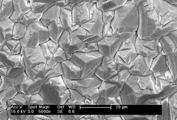
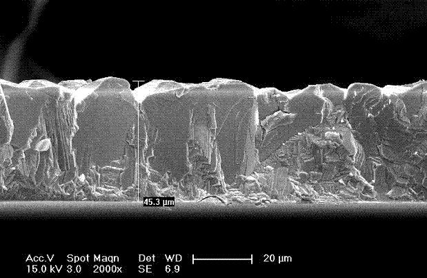
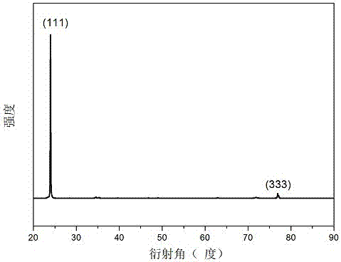
[0022] (3). The growth process of CdZnTe film: turn on the mechanical pump to vacuum, and pump the pressure in the sublimation chamber below 5pa; turn on the halogen lamp to heat the sublimation source and substrate to 600℃ and 550℃ respectively; after 2...


PUM


Abstract

The invention discloses a preparation method of a composite structured GaN / CdZnTe thin film ultraviolet light detector. The preparation method comprises the steps of (1) grinding commercial CdZnTe polycrystal into powder to be used as a sublimation source; (2) taking a monocrystal silicon wafer plated with gallium nitride (GaN) as a substrate, performing blow-drying by nitrogen, and putting into a near space sublimation reaction chamber; (3) pumping air in the sublimation chamber to make the air pressure be 5pa and even below, starting a halogen lamp to heat the sublimation source and the substrate to be 600 DEG C and 550 DEG C; performing growth for 20min, cooling to the room temperature and taking out to obtain a GaN / CdZnTe thin film; and (4) performing metal electrode evaporation on the surface of the GaN / CdZnTe thin film by an evaporation method, then putting the metal electrode into N<2> atmosphere to be annealed to form high ohmic contact between GaN / CdZnTe and the metal electrode, to obtain the composite structured GaN / CdZnTe thin film ultraviolet light detector. By virtue of the GaN substrate adopted in the manufacturing method, it is ensured that the composite structured GaN / CdZnTe thin film ultraviolet light detector can be used in a high-temperature and strong-radiation environment and the detector has high stability and optical response characteristics on ultraviolet light.

Description

Technical field [0001] The invention relates to a method for preparing a GaN / CdZnTe thin film ultraviolet light detector with a composite structure, and belongs to the technical field of inorganic non-metallic material manufacturing technology. Background technique [0002] Ultraviolet detection technology is a new dual-purpose photoelectric detection technology after infrared and laser detection technology. At present, most high-sensitivity ultraviolet light detection uses vacuum photomultiplier tubes that are sensitive to ultraviolet light and similar vacuum-type devices. However, compared with solid-state detection devices, vacuum-type devices have the disadvantages of large volume and high working voltage; for example, silicon photodetection devices are responsive to visible light, and this feature becomes a disadvantage in ultraviolet light detection. At this time, it is required to detect only the ultraviolet signal, which requires expensive pre-filtering facilities. With...

Claims


Application Information

Patent Timeline
Patent Type & Authority Applications(China)
IPC IPC(8): H01L31/109H01L31/0336H01L31/18H01L21/02
CPCH01L21/02389H01L21/02562H01L21/02631H01L31/0336H01L31/109H01L31/18Y02P70/50
Inventor 沈悦张宗坤徐宇豪沈意斌黄健顾峰王林军
Owner SHANGHAI UNIV
Why Eureka
Try Eureka