A non-polar surface quantum dot light-emitting diode and its preparation method

A quantum dot light-emitting, non-polar surface technology, applied in the direction of semiconductor devices, electrical components, circuits, etc., can solve the problems of high dislocation density in the active area, degradation of LEDs performance, and increased quality mismatch, so as to improve the quality of materials , Eliminate the polarization effect and improve the efficiency of the device

Inactive Publication Date: 2019-03-22
INST OF SEMICONDUCTORS - CHINESE ACAD OF SCI
View PDF6 Cites 0 Cited by
  • Summary
  • Abstract
  • Description
  • Claims
  • Application Information

AI Technical Summary

Problems solved by technology

On the one hand, with the increase of In content (from ultraviolet to green light), the lattice mismatch between InGaN with high In content and GaN increases, resulting in a large dislocation density in the active region, and the performance of LEDs based on quantum well luminescence is serious. decline, it is difficult to achieve high-efficiency light emission in the green light band (especially in the 525-575nm wavelength range)
On the other hand, the strong polarization effect induced by the wurtzite crystal structure limits the efficiency improvement of GaN-based materials.

Method used


Image

  • A non-polar surface quantum dot light-emitting diode and its preparation method
  • A non-polar surface quantum dot light-emitting diode and its preparation method
  • A non-polar surface quantum dot light-emitting diode and its preparation method

Examples


preparation example Construction

[0052] The present invention also discloses a method for preparing the above-mentioned non-polar surface quantum dot light-emitting diode, which includes the following steps:

[0053] Step 1, sequentially forming a u-type GaN layer and an n-type GaN layer both on a non-polar surface on the substrate;

[0054] Step 2. First grow a wetting layer on the n-type GaN layer, then grow the non-polar InGaN quantum dots, and then grow the non-polar GaN barrier layer on the InGaN quantum dots; repeat the above steps n times to form active area;

[0055] Step 3, forming a p-type electron blocking layer and a p-type GaN layer both on the non-polar surface on the active region, and completing the preparation of the non-polar surface quantum dot light-emitting diode;

[0056] Among them, n is a natural number.

[0057] In some embodiments of the present invention, the value range of the above n is 3≤n≤15.

[0058] In some embodiments of the present invention, the formation environment of ...

Embodiment 1

[0065] This embodiment provides a non-polar surface quantum dot light-emitting diode structure, which includes the main structure from bottom to top:

[0066] A substrate, the substrate is a (1-102) R-plane sapphire plane or a PSS substrate, and can also be a silicon, silicon carbide, lithium aluminate or GaN homogeneous substrate;

[0067] A stress covariant layer, which is fabricated on the substrate, can be formed by annealing one or more sets of InGaN flexible layers and GaN buffer layers, and has a porous or stripe-like morphology, which can be used to control the growth of GaN on it Layer stress state, other materials that can be made into porous or stripe-like morphology, such as InN, ZnO, AlN or carbon nanorods, can be used as materials for the stress-covariant layer;

[0068] An undoped GaN layer on the non-polar surface, which is fabricated on the stress covariant layer, and the stress state is controlled by the stress covariant layer below it;

[0069] A non-polar ...

Embodiment 2

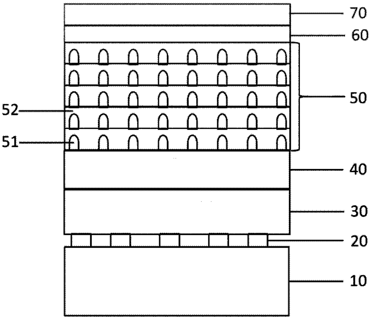
[0084] Such as figure 1 As shown, the present embodiment provides a non-polar surface quantum dot light-emitting diode, including:

[0085] A substrate 10, the substrate 10 is an R-face sapphire substrate of the (1-102) face;

[0086] It should be noted that this embodiment uses a sapphire substrate. For other substrates, such as silicon, silicon carbide or lithium aluminate, as long as the lattice matching degree with the non-polar A-plane GaN is less than 20%, can also be used;

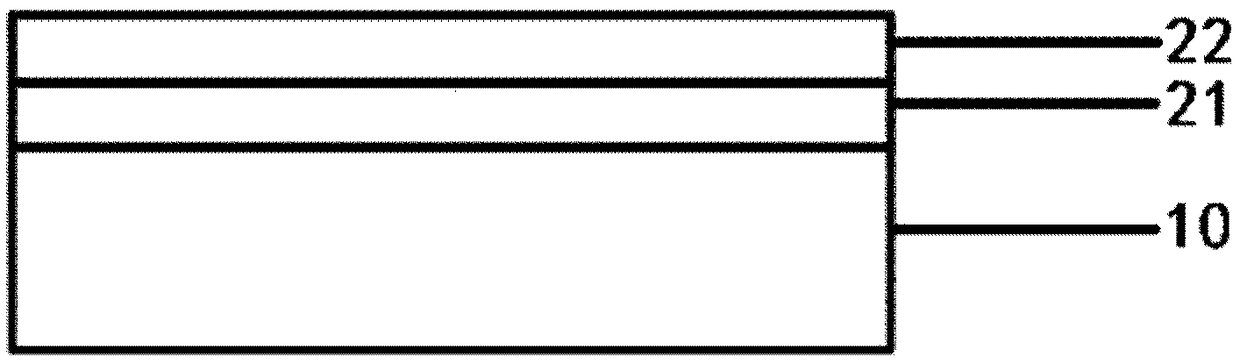
[0087] A stress covariant layer 20 formed by annealing the InGaN flexible layer and the GaN buffer layer, which is fabricated on the substrate 10 . Among them, the thickness of the InGaN flexible layer is 20-100nm, the thickness of the GaN buffer layer is 30-150nm, and the stress-covariant layer formed by annealing has a stripe-like morphology, which can be used to control the stress state of the GaN layer grown on it;

[0088] A non-polar undoped GaN layer 30 is fabricated on the stress-conformi...


PUM


Abstract

The invention provides a non-polar surface quantum dot light-emitting diode, which comprises a substrate, a u-type GaN layer, an n-type GaN layer, an active region, a p-type electron blocking layer and a p-type GaN layer, wherein the u-type GaN layer, the n-type GaN layer, the active region, the p-type electron blocking layer and the p-type GaN layer are laminated on the substrate in sequence and are in non-polar surface; and the active region comprises an InGaN quantum dot potential well layer and a GaN barrier layer in periodic distribution and in non-polar surface. The invention also provides a preparation method of the non-polar surface quantum dot light-emitting diode. By laminating the non-polar surface epitaxial structures on the substrate in sequence, influence of a quantum-confined stark effect on internal quantum efficiency of the device can be eliminated, and a polarization effect can be eliminated effectively; and besides, light wavelength of the light-emitting diode in such crystal orientation can extend to deep green or even orange light area, so that the problem of "green gap" in existing compound semiconductor light-emitting devices can be solved.

Description

technical field [0001] The invention belongs to the technical field of semiconductors, and more specifically relates to a non-polar surface quantum dot light-emitting diode and a preparation method thereof. Background technique [0002] As a typical application of the third-generation wide-bandgap semiconductor technology, commercial GaN-based LEDs have covered the ultraviolet to green light spectrum. As a light-emitting device, GaN-based LEDs can be widely used in many aspects such as indoor and outdoor lighting, commercial lighting, agricultural lighting, traffic lighting, medical lighting, and display backlight. The focus on this light source has greatly improved the preparation technology of GaN-based LEDs in recent years, but some of the technical bottlenecks have become increasingly prominent, and the following two key scientific and technical issues still need to be solved. On the one hand, with the increase of In content (from ultraviolet to green light), the lattic...

Claims


Application Information

Patent Timeline
Patent Type & Authority Patents(China)
IPC IPC(8): H01L33/00H01L33/06H01L33/32
CPCH01L33/0066H01L33/0075H01L33/06H01L33/325
Inventor 赵桂娟汪连山李辉杰孟钰淋吉泽生李方政魏鸿源杨少延王占国
Owner INST OF SEMICONDUCTORS - CHINESE ACAD OF SCI
Why Eureka
Try Eureka