A kind of flexible transparent conductive electrode based on polyimide substrate and preparation method thereof
A transparent conductive electrode, polyimide technology, applied to the conductive layer on the insulating carrier, cable/conductor manufacturing, circuits, etc., can solve the problem of poor adhesion between the metal grid and the substrate, difficult to control the height of the metal grid, High haze and other problems, to achieve the effect of high visible light transmittance, increased light transmittance, and low sheet resistance
- Summary
- Abstract
- Description
- Claims
- Application Information
AI Technical Summary
Problems solved by technology
Method used
Image
Examples
Embodiment 1
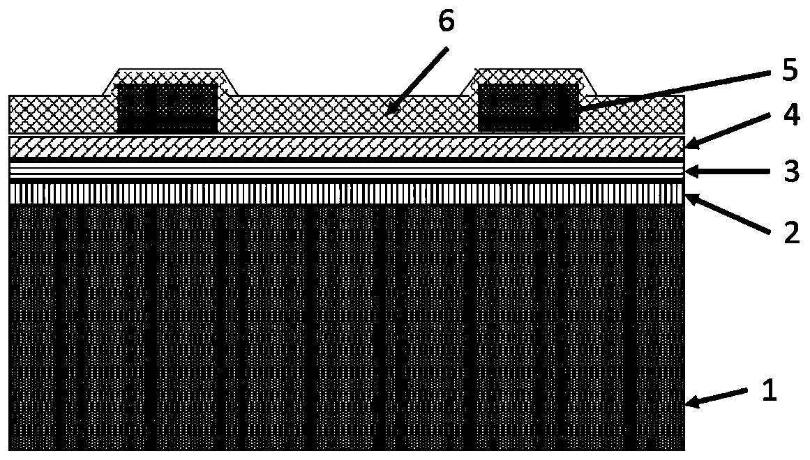
[0036] like figure 1 As shown, it is a schematic structural diagram of a flexible transparent conductive electrode based on a polyimide substrate in the present invention. The polyimide-based flexible transparent conductive electrode in this embodiment includes a polyimide substrate 1 from bottom to top, a wetting layer 2 (also called adhesion layer), metal seed layer 3, second metal layer 4, metal grid layer 5 and zinc oxide anti-reflection layer 6, wetting layer 2 is molybdenum trioxide, metal seed layer 2 is gold, the second The second metal layer is silver, and the metal seed layer 3 and the second metal layer 4 constitute the metal layer. The following are the specific production steps:
[0037] The first step is to successively evaporate MoO on PI by thermal evaporation method. 3 , Au, Ag, thicknesses are 3nm, 2nm, 4nm respectively. In this embodiment, the degree of vacuum during the evaporation process is ≤1.5×10 -4 The thickness of the Pa steamed metal is monitored...
Embodiment 2
[0044] The flexible transparent conductive electrode based on the polyimide substrate of the present invention is manufactured according to the following steps:
[0045] The first step is to successively evaporate MoO on PI by thermal evaporation method. 3 , Au, Ag, thicknesses are 3nm, 2nm, 4nm respectively. In this embodiment, the degree of vacuum during the evaporation process is ≤1.5×10 -4 The thickness of the Pa steamed metal is monitored by a frequency meter.
[0046] In the second step, the metal grid is fabricated by photolithography, evaporation, and lift-off methods. In this example, AZ5214 photoresist is first coated on the PI prepared in the first step, the spin coating is 1000rpm / 3s+3000rpm / 35s, the glue is baked at 112°C / 50s, the MJB4 photolithography machine is exposed for 20s, and the developer Developed to obtain a sample with a photoresist mask pattern, the pattern is a regular hexagon, the side length of the hexagon is 200nm, and the line width of the gri...
Embodiment 3
[0050] The flexible transparent conductive electrode based on the polyimide substrate of the present invention is manufactured according to the following steps:
[0051] In the first step, TiO was deposited on PI by magnetron sputtering by thermal evaporation. 2 , Cu, Ag, thicknesses are 2nm, 1nm, 20nm respectively. In this example sputtered TiO 2 Utilizes 99.999% pure TiO 2 The target material, Cu and Ag, respectively utilize 99.99% pure Cu and Ag targets. The vacuum degree in the process is ≤1.0×10 -6 Torr.
[0052] In the second step, the metal grid is fabricated by photolithography, evaporation, and lift-off methods. In this example, AZ5214 photoresist is first coated on the PI prepared in the first step, the spin coating is 1000rpm / 3s+3000rpm / 35s, the glue is baked at 112°C / 50s, the MJB4 photolithography machine is exposed for 20s, and the developer Developed to obtain a sample with a photoresist mask pattern, the pattern is a regular hexagon, the side length of the...
PUM
| Property | Measurement | Unit |
|---|---|---|
| thickness | aaaaa | aaaaa |
| width | aaaaa | aaaaa |
| thickness | aaaaa | aaaaa |
Abstract
Description
Claims
Application Information


